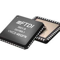
VNC2-48Q1B-REEL FTDI, VNC2-48Q1B-REEL Datasheet - Page 42

VNC2-48Q1B-REEL
Manufacturer Part Number
VNC2-48Q1B-REEL
Description
USB Interface IC Vinculum-II Dual USB Host/Dev IC QFN-48
Manufacturer
FTDI
Type
USB Host/Device Controllerr
Datasheet
1.VNC2-32Q1B-REEL.pdf
(90 pages)
Specifications of VNC2-48Q1B-REEL
Maximum Operating Temperature
+ 85 C
Minimum Operating Temperature
- 40 C
Mounting Style
SMD/SMT
Operating Temperature Range
- 40 C to + 85 C
Supply Current
25 mA
Operating Supply Voltage
1.8 V, 3.3V
Package / Case
QFN-48
Description/function
USB Vinculum-II Dual Host/Dev IC QFN-48
Lead Free Status / RoHS Status
Lead free / RoHS Compliant
Other names
VINCULUM2
- Current page: 42 of 90
- Download datasheet (2Mb)
6.2.1 SPI Clock Phase Modes
SPI interface has 4 unique modes of clock phase (CPHA) and clock polarity (CPOL), known
as Mode 0, Mode 1, Mode 2 and Mode 3. Table 16 summarizes these modes and available interface and
Figure 6-3 is the function timing diagram.
For CPOL = 0, the base (inactive) level of SCLK is 0.
In this mode:
For CPOL =1, the base (inactive) level of SCLK is 1.
In this mode:
Mode
Table 16 - Clock Phase/Polarity Modes
Figure 6-3 - SPI CPOL CPHA Function
0
1
2
3
CPOL
0
0
1
1
• When CPHA = 0, data is clocked in on the rising edge of SCLK, and data is clocked out on
the falling edge of SCLK.
• When CPHA = 1, data is clocked in on the falling edge of SCLK, and data is clocked out on
the rising edge of SCLK
• When CPHA = 0, data v in on the falling edge of SCLK, and data is clocked out on the
rising edge of SCLK
• When CPHA =1, data is clocked in on the rising edge of SCLK, and data is clocked out on
the falling edge of SCLK.
CPHA
0
1
0
1
Copyright © 2010 Future Technology Devices International Limited
Duplex
Full
N
N
Y
Y
VINCULUM-II EMBEDDED DUAL USB HOST CONTROLLER IC Datasheet
Duplex
4 pin
Half
N
Y
N
Y
Duplex
3 pin
Half
N
Y
N
Y
Unmanged
Y
Y
Y
Y
Legacy
VNC1L
N
N
N
N
Document No.: FT_000138
Clearance No.: FTDI#
Version -
143
1.2
42
Related parts for VNC2-48Q1B-REEL
Image
Part Number
Description
Manufacturer
Datasheet
Request
R

Part Number:
Description:
Interface Modules & Development Tools USB to Serial UART MiniB Dev Mod FT232R
Manufacturer:
FTDI
Datasheet:

Part Number:
Description:
BOARD, EVALUATION, EU PSU
Manufacturer:
FTDI
Datasheet:

Part Number:
Description:
BOARD, EVALUATION, UK PSU
Manufacturer:
FTDI
Datasheet:

Part Number:
Description:
BOARD, EVALUATION, US PSU
Manufacturer:
FTDI
Datasheet:

Part Number:
Description:
Specifications: Manufacturer: FTDI ; Product Category: USB Interface IC ; RoHS: Details ; Operating Supply Voltage: 3 V to 5.25 V ; Supply Current: 25 mA ; Maximum Operating Temperature: + 70 C ; Mounting Style: SMD/SMT ; Package / Case: QFN-32
Manufacturer:
FTDI

Part Number:
Description:
integr. usb2.0/uart lqfp32 rohs ftdi reel c1k...
Manufacturer:
FTDI
Datasheet:

Part Number:
Description:
Interface Development Tools USB to UART Breakout Board
Manufacturer:
FTDI
Datasheet:

Part Number:
Description:
IC USB TO SERIAL UART 32-QFN
Manufacturer:
FTDI, Future Technology Devices International Ltd

Part Number:
Description:
USB Interface IC USB to Serial UART Enhanced IC SSOP-28
Manufacturer:
FTDI
Datasheet:

Part Number:
Description:
IC, USB UART INTERFACE, SSOP-28
Manufacturer:
FTDI
Datasheet:

Part Number:
Description:
IC, USB UART INTERFACE, QFN-32
Manufacturer:
FTDI
Datasheet:

Part Number:
Description:
IC, USB FIFO INTERFACE, SSOP-28
Manufacturer:
FTDI
Datasheet:

Part Number:
Description:
MODULE, USB, 4 PORT, FT4232H BASED
Manufacturer:
FTDI
Datasheet:

Part Number:
Description:
357-036-542-201 CARDEDGE 36POS DL .156 BLK LOPRO
Manufacturer:
FTDI
Datasheet:

Part Number:
Description:
357-036-542-201 CARDEDGE 36POS DL .156 BLK LOPRO
Manufacturer:
FTDI
Datasheet:


