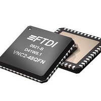
VNC2-48Q1B-REEL FTDI, VNC2-48Q1B-REEL Datasheet - Page 41

VNC2-48Q1B-REEL
Manufacturer Part Number
VNC2-48Q1B-REEL
Description
USB Interface IC Vinculum-II Dual USB Host/Dev IC QFN-48
Manufacturer
FTDI
Type
USB Host/Device Controllerr
Datasheet
1.VNC2-32Q1B-REEL.pdf
(90 pages)
Specifications of VNC2-48Q1B-REEL
Maximum Operating Temperature
+ 85 C
Minimum Operating Temperature
- 40 C
Mounting Style
SMD/SMT
Operating Temperature Range
- 40 C to + 85 C
Supply Current
25 mA
Operating Supply Voltage
1.8 V, 3.3V
Package / Case
QFN-48
Description/function
USB Vinculum-II Dual Host/Dev IC QFN-48
Lead Free Status / RoHS Status
Lead free / RoHS Compliant
Other names
VINCULUM2
6.2 Serial Peripheral Interface – SPI Modes
The Serial Peripheral Interface Bus is an industry standard communications interface. Devices
communicate in Master / Slave mode, with the Master initiating the data transfer.
VNC2 has one master module and two slave modules. Each SPI slave module has four signals – clock,
slave select, MOSI (master out – slave in) and MISO (master in – slave out). The SPI Master has the
same four signals as the slave modules but with one additional signal because it requires a slave select
for the second slave module. Table 14 lists how the signals are named in each module.
The SPI Master clock can operate up to one half of the CPU system clock depending on what power mode
the device is set to:
Table 14 SPI Signal Names
The SPI slave protocol by default does not support any form of handshaking. FTDI have added extra
modes to support handshaking, faster throughput of data and reduced pin count. There are 5 modes
(Table 15) of operation in the VNC2 SPI Slave.
Table 15 - SPI Slave Speeds
VNC2 SPI Master is described in Section 6.4.1 SPI Master Signal Descriptions.
Table 17
the package size. Further details on the configuration of input and output signals are available in Section
5 -
SPI Slave
SPI Slave
Half Duplex 4
Half Duplex 3
Module
Master
Unmanaged
Full Duplex
SPI
I/O Multiplexer
0
1
VNC1L
Mode
pin
pin
Normal power mode 48Mhz would set the SPI maximum clock to 24Mhz
Low power mode 24Mhz would set the SPI maximum clock to 12Mhz
Lowest power mode 12Mhz would set the SPI maximum clock to 6hMz
shows the SPI master signals and the available pins that they can be mapped to depending on
spi_m_ss_0#
spi_m_ss_1#
Signal Name
spi_s0_mosi
spi_s0_miso
spi_s1_mosi
spi_s1_miso
spi_m_mosi
spi_m_miso
spi_s0_ss#
spi_s1_ss#
spi_s0_clk
spi_s1_clk
spi_m_clk
Full Duplex – Section 6.3.2
Half Duplex, 4 pin - Section 6.3.3
Half Duplex, 3 pin - Section 6.3.4
Unmanaged - Section 6.3.5
VNC1L legacy mode – Section 6.3.6
.
Copyright © 2010 Future Technology Devices International Limited
Pins
4
4
4
3
4
VINCULUM-II EMBEDDED DUAL USB HOST CONTROLLER IC Datasheet
Output
Output
Output
Output
Output
Output
Input
Input
Input
Input
Input
Input
Input
Type
Word Size
Description
Clock input – slave 0
Active low chip select input – slave 0
Master out serial in – slave 0
Master in slave out – slave 0
Clock input – slave 1
Active low chip select input – slave 1
Master out slave in – slave 1
Master in slave out – slave 1
Clock output – master
Master out slave in - master
Master in slave out - master
Active low slave select 0 from master to slave 0
Active low slave select 1 from master to slave 1
12
8
8
8
8
Handshaking
Yes
Yes
Yes
Yes
No
Write 100%
Write 100%
Write 100%
Read 100%
Read 100%
Write 66%
Write 50%
Read 66%
Read 50%
Read 50%
Document No.: FT_000138
Clearance No.: FTDI#
Speed
MOSI becomes
MOSI becomes
Version -
bi-directional
bi-directional
Legacy mode
Comments
143
1.2
41


