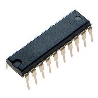
ATTINY861-20PU Atmel, ATTINY861-20PU Datasheet - Page 148

ATTINY861-20PU
Manufacturer Part Number
ATTINY861-20PU
Description
Microcontrollers (MCU) 8kB Flash 0.512kB EEPROM 16 I/O Pins
Manufacturer
Atmel
Specifications of ATTINY861-20PU
Processor Series
ATTINY8x
Core
AVR8
Data Bus Width
8 bit
Data Ram Size
512 B
Interface Type
2-Wire/SPI/USI
Maximum Clock Frequency
20 MHz
Number Of Programmable I/os
16
Number Of Timers
2
Operating Supply Voltage
2.7 V to 5.5 V
Maximum Operating Temperature
+ 85 C
Mounting Style
Through Hole
3rd Party Development Tools
EWAVR, EWAVR-BL
Development Tools By Supplier
ATAVRDRAGON, ATSTK500, ATSTK600, ATAVRISP2, ATAVRONEKIT, ATAVRMC320
Minimum Operating Temperature
- 40 C
On-chip Adc
11-ch x 10-bit
Program Memory Type
Flash
Program Memory Size
8 KB
Package / Case
PDIP-20
Controller Family/series
AVR Tiny
Core Size
8 Bit
No. Of I/o's
16
Eeprom Memory Size
512Byte
Ram Memory Size
512Byte
Cpu Speed
20MHz
No. Of Timers
2
Rohs Compliant
Yes
Package
20PDIP
Device Core
AVR
Family Name
ATtiny
Maximum Speed
20 MHz
Ram Size
512 Byte
Operating Temperature
-40 to 85 °C
Lead Free Status / RoHS Status
Lead free / RoHS Compliant
Available stocks
Company
Part Number
Manufacturer
Quantity
Price
Company:
Part Number:
ATTINY861-20PU
Manufacturer:
Atmel
Quantity:
135
Company:
Part Number:
ATTINY861-20PU ES
Manufacturer:
ATMEL
Quantity:
215
- Current page: 148 of 242
- Download datasheet (5Mb)
15.6
148
Changing Channel or Reference Selection
ATtiny261/461/861
Figure 15-7. ADC Timing Diagram, Free Running Conversion
For a summary of conversion times, see
Table 15-1.
The MUX5:0 and REFS2:0 bits in the ADCSRB and ADMUX registers are single buffered
through a temporary register to which the CPU has random access. This ensures that the chan-
nels and reference selection only takes place at a safe point during the conversion. The channel
and reference selection is continuously updated until a conversion is started. Once the conver-
sion starts, the channel and reference selection is locked to ensure a sufficient sampling time for
the ADC. Continuous updating resumes in the last ADC clock cycle before the conversion com-
pletes (ADIF in ADCSRA is set). Note that the conversion starts on the following rising ADC
clock edge after ADSC is written. The user is thus advised not to write new channel or reference
selection values to ADMUX until one ADC clock cycle after ADSC is written.
If Auto Triggering is used, the exact time of the triggering event can be indeterministic. Special
care must be taken when updating the ADMUX Register, in order to control which conversion
will be affected by the new settings.
If both ADATE and ADEN is written to one, an interrupt event can occur at any time. If the
ADMUX Register is changed in this period, the user cannot tell if the next conversion is based
on the old or the new settings.
ADMUX can be safely updated in the following ways:
Condition
First conversion
Normal conversions
Auto Triggered conversions
ADC Conversion Time
Cycle Number
ADC Clock
ADSC
ADIF
ADCH
ADCL
Conversion
Sample & Hold
(Cycles from Start of Conversion)
Complete
One Conversion
11
12
Table
13.5
1.5
13
2
15-1.
Next Conversion
1
Sign and MSB of Result
LSB of Result
2
MUX and REFS
Update
3
Sample & Hold
Total Conversion Time (Cycles)
4
13.5
25
13
2588E–AVR–08/10
Related parts for ATTINY861-20PU
Image
Part Number
Description
Manufacturer
Datasheet
Request
R

Part Number:
Description:
Manufacturer:
Atmel Corporation
Datasheet:

Part Number:
Description:
Manufacturer:
Atmel Corporation
Datasheet:

Part Number:
Description:
IC MCU AVR 8K FLASH 20MHZ 32-QFN
Manufacturer:
Atmel
Datasheet:

Part Number:
Description:
IC MCU AVR 8K FLASH 20MHZ 20SOIC
Manufacturer:
Atmel
Datasheet:

Part Number:
Description:
MCU AVR 8K FLASH 15MHZ 32-QFN
Manufacturer:
Atmel
Datasheet:

Part Number:
Description:
MCU AVR 8K FLASH 15MHZ 20-SOIC
Manufacturer:
Atmel
Datasheet:

Part Number:
Description:
MCU AVR 8KB FLASH 15MHZ 32-VQFN
Manufacturer:
Atmel
Datasheet:

Part Number:
Description:
8-bit Microcontrollers - MCU 8KB FL 512B EE 512B SRAM 20MHZ IND 5V
Manufacturer:
Atmel

Part Number:
Description:
IC, MCU, 8BIT, 2K FLASH, 20SOIC
Manufacturer:
Atmel
Datasheet:

Part Number:
Description:
IC, MCU, 8BIT, 2K FLASH, 20PDIP
Manufacturer:
Atmel
Datasheet:


