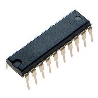
ATTINY861-20PU Atmel, ATTINY861-20PU Datasheet - Page 175

ATTINY861-20PU
Manufacturer Part Number
ATTINY861-20PU
Description
Microcontrollers (MCU) 8kB Flash 0.512kB EEPROM 16 I/O Pins
Manufacturer
Atmel
Specifications of ATTINY861-20PU
Processor Series
ATTINY8x
Core
AVR8
Data Bus Width
8 bit
Data Ram Size
512 B
Interface Type
2-Wire/SPI/USI
Maximum Clock Frequency
20 MHz
Number Of Programmable I/os
16
Number Of Timers
2
Operating Supply Voltage
2.7 V to 5.5 V
Maximum Operating Temperature
+ 85 C
Mounting Style
Through Hole
3rd Party Development Tools
EWAVR, EWAVR-BL
Development Tools By Supplier
ATAVRDRAGON, ATSTK500, ATSTK600, ATAVRISP2, ATAVRONEKIT, ATAVRMC320
Minimum Operating Temperature
- 40 C
On-chip Adc
11-ch x 10-bit
Program Memory Type
Flash
Program Memory Size
8 KB
Package / Case
PDIP-20
Controller Family/series
AVR Tiny
Core Size
8 Bit
No. Of I/o's
16
Eeprom Memory Size
512Byte
Ram Memory Size
512Byte
Cpu Speed
20MHz
No. Of Timers
2
Rohs Compliant
Yes
Package
20PDIP
Device Core
AVR
Family Name
ATtiny
Maximum Speed
20 MHz
Ram Size
512 Byte
Operating Temperature
-40 to 85 °C
Lead Free Status / RoHS Status
Lead free / RoHS Compliant
Available stocks
Company
Part Number
Manufacturer
Quantity
Price
Company:
Part Number:
ATTINY861-20PU
Manufacturer:
Atmel
Quantity:
135
Company:
Part Number:
ATTINY861-20PU ES
Manufacturer:
ATMEL
Quantity:
215
- Current page: 175 of 242
- Download datasheet (5Mb)
18.6.2
2588E–AVR–08/10
Serial Programming Instruction set
Table 18-10. Minimum Wait Delay Before Writing the Next Flash or EEPROM Location
The instruction set is described in
Symbol
t
t
t
t
5. A: The EEPROM array is programmed one byte at a time by supplying the address and
6. Any memory location can be verified by using the Read instruction which returns the
7. At the end of the programming session, RESET can be set high to commence normal
8. Power-off sequence (if needed):
WD_FLASH
WD_EEPROM
WD_ERASE
WD_FUSE
interface before the Flash write operation completes can result in incorrect
programming.
data together with the appropriate Write instruction. An EEPROM memory location is
first automatically erased before new data is written. If polling (RDY/BSY) is not used,
the user must wait at least t
In a chip erased device, no 0xFFs in the data file(s) need to be programmed.
B: The EEPROM array is programmed one page at a time. The Memory page is loaded
one byte at a time by supplying the 2 LSB of the address and data together with the
Load EEPROM Memory Page instruction. The EEPROM Memory Page is stored by
loading the Write EEPROM Memory Page Instruction with the 6 MSB of the address.
When using EEPROM page access only byte locations loaded with the Load EEPROM
Memory Page instruction is altered. The remaining locations remain unchanged. If poll-
ing (RDY/BSY) is not used, the used must wait at least t
next page (See
be programmed.
content at the selected address at serial output MISO.
operation.
Set RESET to “1”.
Turn V
CC
power off.
Table
18-8). In a chip erased device, no 0xFF in the data file(s) need to
WD_EEPROM
Table 18-11 on page 176
before issuing the next byte. (See
Minimum Wait Delay
and
WD_EEPROM
4.5 ms
4.0 ms
9.0 ms
4.5 ms
Figure 18-2 on page
before issuing the
Table
18-10.)
177.
175
Related parts for ATTINY861-20PU
Image
Part Number
Description
Manufacturer
Datasheet
Request
R

Part Number:
Description:
Manufacturer:
Atmel Corporation
Datasheet:

Part Number:
Description:
Manufacturer:
Atmel Corporation
Datasheet:

Part Number:
Description:
IC MCU AVR 8K FLASH 20MHZ 32-QFN
Manufacturer:
Atmel
Datasheet:

Part Number:
Description:
IC MCU AVR 8K FLASH 20MHZ 20SOIC
Manufacturer:
Atmel
Datasheet:

Part Number:
Description:
MCU AVR 8K FLASH 15MHZ 32-QFN
Manufacturer:
Atmel
Datasheet:

Part Number:
Description:
MCU AVR 8K FLASH 15MHZ 20-SOIC
Manufacturer:
Atmel
Datasheet:

Part Number:
Description:
MCU AVR 8KB FLASH 15MHZ 32-VQFN
Manufacturer:
Atmel
Datasheet:

Part Number:
Description:
8-bit Microcontrollers - MCU 8KB FL 512B EE 512B SRAM 20MHZ IND 5V
Manufacturer:
Atmel

Part Number:
Description:
IC, MCU, 8BIT, 2K FLASH, 20SOIC
Manufacturer:
Atmel
Datasheet:

Part Number:
Description:
IC, MCU, 8BIT, 2K FLASH, 20PDIP
Manufacturer:
Atmel
Datasheet:


