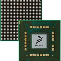
MPC8536BVTAVL Freescale Semiconductor, MPC8536BVTAVL Datasheet - Page 24

MPC8536BVTAVL
Manufacturer Part Number
MPC8536BVTAVL
Description
Microprocessors (MPU) 8536 INDUSTRIAL 1500
Manufacturer
Freescale Semiconductor
Datasheet
1.MPC8536EBVTAQG.pdf
(126 pages)
Specifications of MPC8536BVTAVL
Processor Series
MPC85xx
Core
e500
Data Bus Width
32 bit
Maximum Clock Frequency
1500 MHz
Operating Supply Voltage
3.3 V
Maximum Operating Temperature
+ 105 C
Mounting Style
SMD/SMT
Interface Type
I2C, SPI, UART
Minimum Operating Temperature
0 C
Package / Case
FCPBGA-783
Lead Free Status / RoHS Status
Lead free / RoHS Compliant
Available stocks
Company
Part Number
Manufacturer
Quantity
Price
Company:
Part Number:
MPC8536BVTAVLA
Manufacturer:
Freescale Semiconductor
Quantity:
135
Company:
Part Number:
MPC8536BVTAVLA
Manufacturer:
Freescale Semiconductor
Quantity:
10 000
Overall DC Electrical Characteristics
Figure 2
The core voltage must always be provided at nominal 1.0 V . (See
processor interface I/Os are provided through separate sets of supply pins and must be provided at the voltages shown in
The input voltage threshold scales with respect to the associated I/O supply voltage. OV
CMOS I/O circuits and satisfy appropriate LVCMOS type specifications. The DDR2 and DDR3 SDRAM interface uses
differential receivers referenced by the externally supplied MV
SSTL_1.8 electrical signaling standard for DDR2 or 1.5-V electrical signaling for DDR3. The DDR DQS receivers cannot be
operated in single-ended fashion. The complement signal must be properly driven and cannot be grounded.
24
shows the undershoot and overshoot voltages at the interfaces of the MPC8535E.
V
IH
MPC8535E PowerQUICC III Integrated Processor Hardware Specifications, Rev. 3
V
Note:
1. t
2. With the PCI overshoot allowed (as specified above), the device
IL
Figure 7. Overshoot/Undershoot Voltage for GV
B/G/L/OV
For I
For DDR, t
For eTSEC, t
For eLBC, t
For PCI, t
does not fully comply with the maximum AC ratings and device protection
guideline outlined in the PCI rev. 2.2 standard (section 4.2.2.3).
CLOCK
B/G/L/OV
2
C and JTAG, t
GND – 0.3 V
GND – 0.7 V
B/G/L/OV
refers to the clock period associated with the respective interface:
DD
CLOCK
DD
CLOCK
CLOCK
+ 20%
CLOCK
+ 5%
GND
DD
references PCI1_CLK or SYSCLK.
references MCLK.
references LCLK.
CLOCK
references EC_GTX_CLK125.
references SYSCLK.
REF
Table 2
n signal (nominally set to GV
Not to Exceed 10%
of t
for actual recommended core voltage). Voltage to the
CLOCK
1
DD
/OV
DD
and LV
DD
/LV
DD
DD
DD
/2) as is appropriate for the
based receivers are simple
Freescale Semiconductor
Table
2.


