MPC8536BVTAVL Freescale Semiconductor, MPC8536BVTAVL Datasheet - Page 31
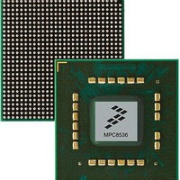
MPC8536BVTAVL
Manufacturer Part Number
MPC8536BVTAVL
Description
Microprocessors (MPU) 8536 INDUSTRIAL 1500
Manufacturer
Freescale Semiconductor
Datasheet
1.MPC8536EBVTAQG.pdf
(126 pages)
Specifications of MPC8536BVTAVL
Processor Series
MPC85xx
Core
e500
Data Bus Width
32 bit
Maximum Clock Frequency
1500 MHz
Operating Supply Voltage
3.3 V
Maximum Operating Temperature
+ 105 C
Mounting Style
SMD/SMT
Interface Type
I2C, SPI, UART
Minimum Operating Temperature
0 C
Package / Case
FCPBGA-783
Lead Free Status / RoHS Status
Lead free / RoHS Compliant
Available stocks
Company
Part Number
Manufacturer
Quantity
Price
Company:

Part Number:
MPC8536BVTAVLA
Manufacturer:
Freescale Semiconductor
Quantity:
135
Company:
Part Number:
MPC8536BVTAVLA
Manufacturer:
Freescale Semiconductor
Quantity:
10 000


2.6
This section describes the DC and AC electrical specifications for the DDR SDRAM interface of the MPC8535E. Note that
DDR2 SDRAM is GV
2.6.1
Table 12
interfacing to DDR2 SDRAM.
Table 13
to DDR3 SDRAM.
Freescale Semiconductor
I/O supply voltage
I/O reference voltage
I/O termination voltage
Input high voltage
Input low voltage
Output leakage current
Output high current (V
Output low current (V
Notes:
1. GV
2. MV
3. V
4. Output leakage is measured with all outputs disabled, 0 V
I/O supply voltage
I/O reference voltage
Input high voltage
Input low voltage
Output leakage current
Notes:
1. GV
2. MV
3. Output leakage is measured with all outputs disabled, 0 V
Peak-to-peak noise on MV
equal to MV
Peak-to-peak noise on MV
TT
DD
REF
DD
REF
is not applied directly to the device. It is the supply to which far end signal termination is made and is expected to be
provides the recommended operating conditions for the DDR SDRAM Controller of the MPC8535E when interfacing
provides the recommended operating conditions for the DDR SDRAM component(s) of the MPC8535E when
is expected to be within 50 mV of the DRAM GV
is expected to be within 50 mV of the DRAM GV
DDR2 and DDR3 SDRAM
is expected to be equal to 0.5 × GV
n is expected to be equal to 0.5 × GV
Parameter/Condition
Parameter/Condition
Table 13. DDR3 SDRAM Interface DC Electrical Characteristics for GV
DDR2 and DDR3 SDRAM DC Electrical Characteristics
REF
Table 12. DDR2 SDRAM DC Electrical Characteristics for GV
. This rail should track variations in the DC level of MV
MPC8535E PowerQUICC III Integrated Processor Hardware Specifications, Rev. 3
DD
OUT
OUT
(type) = 1.8 V and DDR3 SDRAM is GV
= 0.280 V)
= 1.420 V)
REF
REF
n may not exceed ±1% of the DC value.
may not exceed ±2% of the DC value.
DD
DD
Symbol
, and to track GV
MV
Symbol
MV
GV
GV
, and to track GV
V
V
I
V
I
I
OZ
OH
V
V
I
OL
TT
OZ
REF
IH
IL
REF
DD
IH
IL
DD
n
DD
DD
at all times.
≤
MV
at all times.
≤
MV
MV
0.49 × GV
V
0.49 × GV
V
OUT
REF
DD
OUT
REF
DD
REF
–13.4
1.425
GND
DD
–0.3
13.4
Min
Min
–50
–50
1.7
n + 0.100
DC variations as measured at the receiver.
(type) = 1.5 V.
≤
+ 0.125
≤
– 0.04
DC variations as measured at the receiver.
GV
GV
REF
DD
DD
DD
DD
.
.
.
MV
MV
MV
0.51 × GV
0.51 × GV
REF
GV
REF
REF
GV
1.575
Max
DD
n – 0.100
Max
50
DD
1.9
50
—
—
DD
– 0.125
+ 0.04
+ 0.3
(typ) = 1.8 V
DD
DD
DD
(typ) = 1.5 V
DDR2 and DDR3 SDRAM
Unit
Unit
μA
mA
mA
μA
V
V
V
V
V
V
V
V
V
Notes
Notes
—
—
—
—
—
—
1
2
3
1
2
3
4
31
Related parts for MPC8536BVTAVL
Image
Part Number
Description
Manufacturer
Datasheet
Request
R

Part Number:
Description:
BOARD REF COMEXPRESS MPC8536
Manufacturer:
Freescale Semiconductor
Datasheet:

Part Number:
Description:
MCU, MPU & DSP Development Tools COMEXPRESS BASED MPC8536
Manufacturer:
Freescale Semiconductor
Datasheet:

Part Number:
Description:
Manufacturer:
Freescale Semiconductor, Inc
Datasheet:
Part Number:
Description:
Manufacturer:
Freescale Semiconductor, Inc
Datasheet:
Part Number:
Description:
Manufacturer:
Freescale Semiconductor, Inc
Datasheet:
Part Number:
Description:
Manufacturer:
Freescale Semiconductor, Inc
Datasheet:
Part Number:
Description:
Manufacturer:
Freescale Semiconductor, Inc
Datasheet:
Part Number:
Description:
Manufacturer:
Freescale Semiconductor, Inc
Datasheet:
Part Number:
Description:
Manufacturer:
Freescale Semiconductor, Inc
Datasheet:
Part Number:
Description:
Manufacturer:
Freescale Semiconductor, Inc
Datasheet:
Part Number:
Description:
Manufacturer:
Freescale Semiconductor, Inc
Datasheet:
Part Number:
Description:
Manufacturer:
Freescale Semiconductor, Inc
Datasheet:
Part Number:
Description:
Manufacturer:
Freescale Semiconductor, Inc
Datasheet:
Part Number:
Description:
Manufacturer:
Freescale Semiconductor, Inc
Datasheet:
Part Number:
Description:
Manufacturer:
Freescale Semiconductor, Inc
Datasheet: