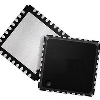
ispPAC-POWR607-01SN32I Lattice, ispPAC-POWR607-01SN32I Datasheet - Page 18

ispPAC-POWR607-01SN32I
Manufacturer Part Number
ispPAC-POWR607-01SN32I
Description
Supervisory Circuits Prec Prog Pwr Supply Seq Mon IND
Manufacturer
Lattice
Type
Power Supply Sequencer and Monitorr
Series
ispPAC®r
Datasheet
1.ISPPAC-POWR607-01SN32I.pdf
(28 pages)
Specifications of ispPAC-POWR607-01SN32I
Internal Hysteresis
Yes
Minimum Operating Temperature
- 40 C
Output Type
Open Collector / Drain
Power Fail Detection
Yes
Number Of Voltages Monitored
6
Monitored Voltage
Adj V
Undervoltage Threshold
Adj
Overvoltage Threshold
Adj
Manual Reset
Resettable
Watchdog
Yes
Power-up Reset Delay (typ)
100 us
Supply Voltage (max)
3.96 V
Supply Voltage (min)
2.64 V
Supply Current (typ)
3.5 mA
Mounting Style
SMD/SMT
Maximum Operating Temperature
+ 85 C
Package / Case
QFN-32
Applications
General Purpose
Voltage - Input
-0.3 V ~ 5.9 V
Voltage - Supply
2.64 V ~ 3.96 V
Current - Supply
3.5mA
Operating Temperature
-40°C ~ 85°C
Mounting Type
Surface Mount
Lead Free Status / RoHS Status
Lead free / RoHS Compliant
Available stocks
Company
Part Number
Manufacturer
Quantity
Price
Company:
Part Number:
ISPPAC-POWR607-01SN32I
Manufacturer:
LATTICE
Quantity:
284
Part Number:
ISPPAC-POWR607-01SN32I
Manufacturer:
LATTICE
Quantity:
20 000
Lattice Semiconductor
ispPAC-POWR607 Data Sheet
accommodate the load voltage at the FET’s source, when the source pin of the FET is tied to the supply of the tar-
get board. When the HVOUT pin is sourcing current (charging a FET gate) the source current is 15µA. When the
driver is turned to the off state, the driver will sink current to ground, and this sink current is typically 2.5mA (1mA
min.) to quickly turn off the FET.
During initial power up and for short periods of time during programming, the HVOUTx pins will assume a high
impedance output configuration (Hi-Z). This occurs whether the pin is configured as a high voltage MOSFET driver
2
or as an open drain output. It happens due to the period of uncertainty before the E
CMOS memory is resolved at
initial turn on and whenever being re-programmed. To insure any FETs controlled by ispPAC-POWR607 HVOUTx
pins are always off during these times, place a 10MΩ (min) resistor between each HVOUTx pin and ground. Since
this will subtract less than 1uA from the total drive capability of the HVOUT pin in FET driver mode, it will have a
negligible affect on its specified drive performance.
Software-Based Design Environment
Designers can configure the ispPAC-POWR607 using PAC-Designer, an easy to use, Microsoft Windows compati-
ble program. Circuit designs are entered graphically and then verified, all within the PAC-Designer environment.
Full device programming is supported using PC parallel port I/O operations and a download cable connected to the
serial programming interface pins of the ispPAC-POWR607. A library of configurations is included with basic solu-
tions and examples of advanced circuit techniques are available on the Lattice web site for downloading. In addi-
tion, comprehensive on-line and printed documentation is provided that covers all aspects of PAC-Designer
operation. The PAC-Designer schematic window, shown in Figure 4-15, provides access to all configurable ispPAC-
POWR607 elements via its graphical user interface. All analog input and output pins are represented. Static or non-
configurable pins such as power, ground, and the serial digital interface are omitted for clarity. Any element in the
schematic window can be accessed via mouse operations as well as menu commands. When completed, configu-
rations can be saved, simulated, and downloaded to devices.
Figure 4-15. PAC-Designer ispPAC-POWR607 Design Entry Screen
4-18


