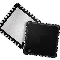
ispPAC-POWR607-01SN32I Lattice, ispPAC-POWR607-01SN32I Datasheet - Page 24

ispPAC-POWR607-01SN32I
Manufacturer Part Number
ispPAC-POWR607-01SN32I
Description
Supervisory Circuits Prec Prog Pwr Supply Seq Mon IND
Manufacturer
Lattice
Type
Power Supply Sequencer and Monitorr
Series
ispPAC®r
Datasheet
1.ISPPAC-POWR607-01SN32I.pdf
(28 pages)
Specifications of ispPAC-POWR607-01SN32I
Internal Hysteresis
Yes
Minimum Operating Temperature
- 40 C
Output Type
Open Collector / Drain
Power Fail Detection
Yes
Number Of Voltages Monitored
6
Monitored Voltage
Adj V
Undervoltage Threshold
Adj
Overvoltage Threshold
Adj
Manual Reset
Resettable
Watchdog
Yes
Power-up Reset Delay (typ)
100 us
Supply Voltage (max)
3.96 V
Supply Voltage (min)
2.64 V
Supply Current (typ)
3.5 mA
Mounting Style
SMD/SMT
Maximum Operating Temperature
+ 85 C
Package / Case
QFN-32
Applications
General Purpose
Voltage - Input
-0.3 V ~ 5.9 V
Voltage - Supply
2.64 V ~ 3.96 V
Current - Supply
3.5mA
Operating Temperature
-40°C ~ 85°C
Mounting Type
Surface Mount
Lead Free Status / RoHS Status
Lead free / RoHS Compliant
Available stocks
Company
Part Number
Manufacturer
Quantity
Price
Company:
Part Number:
ISPPAC-POWR607-01SN32I
Manufacturer:
LATTICE
Quantity:
284
Part Number:
ISPPAC-POWR607-01SN32I
Manufacturer:
LATTICE
Quantity:
20 000
Lattice Semiconductor
IDCODE – This instruction connects the output of the Identification Code Data Shift (IDCODE) Register to TDO
(Figure 4-20), to support reading out the identification code.
Figure 4-20. IDCODE Register
PROGRAM_DISABLE – This instruction disables the programming mode of the ispPAC-POWR607. The Test-
Logic-Reset JTAG state can also be used to cancel the programming mode of the ispPAC-POWR607.
UES_READ – This instruction both reads the E
between the TDI and TDO pins (as shown in Figure 4-17), to support programming or reading of the user electronic
signature bits.
Figure 4-21. UES Register
UES_PROGRAM – This instruction will program the content of the UES Register into the UES E
The device must already be in programming mode (PROGRAM_ENABLE instruction). This instruction also forces
the outputs into the OUTPUTS_HIGHZ.
ERASE_DONE_BIT – This instruction clears the ‘Done’ bit, which prevents the ispPAC-POWR607 sequence from
starting.
PROGRAM_DONE_BIT – This instruction sets the ‘Done’ bit, which enables the ispPAC-POWR607 sequence to
start.
RESET – This instruction resets the PLD sequence and output macrocells. The condition of the ispPAC-POWR607
is the same as initial turn-on after POR is completed.
PLD_VERIFY_INCR – This instruction reads out the PLD data register for the current address and increments the
address register for the next read.
Notes:
In all of the descriptions above, OUTPUTS_HIGHZ refers both to the instruction and the state of the digital and
FET driver output pins, in which all are tri-stated.
Before any of the above programming instructions are executed, the respective E
using the corresponding erase instruction.
Bit
31
Bit
15
Bit
30
Bit
14
Bit
29
Bit
13
Bit
28
Bit
12
Bit
27
Bit
11
2
CMOS bits into the UES register and places the UES register
4-24
Bit
Bit
4
4
Bit
Bit
3
3
ispPAC-POWR607 Data Sheet
Bit
Bit
2
2
2
CMOS bits need to be erased
Bit
Bit
1
1
2
Bit
Bit
0
CMOS memory.
0
TDO
TDO


