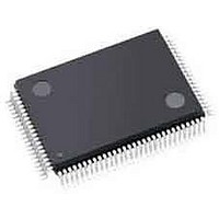
A54SX08A-TQG100 Actel, A54SX08A-TQG100 Datasheet - Page 106

A54SX08A-TQG100
Manufacturer Part Number
A54SX08A-TQG100
Description
FPGA - Field Programmable Gate Array 12K System Gates
Manufacturer
Actel
Datasheet
1.A54SX08A-TQG100.pdf
(108 pages)
Specifications of A54SX08A-TQG100
Processor Series
A54SX08
Core
IP Core
Number Of Macrocells
512
Maximum Operating Frequency
350 MHz
Number Of Programmable I/os
130
Delay Time
4 ns to 8.4 ns
Supply Voltage (max)
5.25 V
Maximum Operating Temperature
+ 70 C
Minimum Operating Temperature
0 C
Development Tools By Supplier
Silicon-Explorer II, Silicon-Sculptor 3, SI-EX-TCA
Mounting Style
SMD/SMT
Supply Voltage (min)
2.25 V
Number Of Gates
8000
Package / Case
TQFP-100
Lead Free Status / RoHS Status
Lead free / RoHS Compliant
Available stocks
Company
Part Number
Manufacturer
Quantity
Price
Company:
Part Number:
A54SX08A-TQG100
Manufacturer:
Microsemi SoC
Quantity:
10 000
Part Number:
A54SX08A-TQG100
Manufacturer:
MICROSEMI/美高森美
Quantity:
20 000
Company:
Part Number:
A54SX08A-TQG100A
Manufacturer:
Microsemi SoC
Quantity:
10 000
Company:
Part Number:
A54SX08A-TQG100I
Manufacturer:
Microsemi SoC
Quantity:
10 000
4 -2
Previous Version Changes in Current Version (v5 . 3)
SX-A Family FPGAs
(continued)
v2.0.1
v4.0
v3.0
Table 2-12
The was updated.
The
Table 2-13
Table 2-13
All timing tables were updated.
The
Design Theft" section
The
The
The
The
The
The
The
The
The
The
The
The
The
The
The
The
The
The
The
The
The
The
The
The
The
The
The
numbers.
"Sample Path Calculations"
"Ordering Information" section
"Temperature Grade Offering" section
Figure 1-1 • SX-A Family Interconnect Elements
“"Clock Resources"
Table 1-1 • SX-A Clock Resources
"User Security" section
"I/O Modules" section
Table 1-2 • I/O Features
Table 1-3 • I/O Characteristics for All I/O Configurations
Table 1-4 • Power-Up Time at which I/Os Become Active
Figure 1-12 • Device Selection Wizard
"Boundary-Scan Pin Configurations and Functions" section
Table 1-9 • Device Configuration Options for Probe Capability (TRST Pin Reserved)
"SX-A Probe Circuit Control Pins" section
"Design Considerations" section
Figure 1-13 • Probe Setup
Design Environment
Figure 1-13 • Design Flow
"Absolute Maximum Ratings*" section
"Recommended Operating Conditions" section
"Electrical Specifications" section
"2.5V LVCMOS2 Electrical Specifications" section
"SX-A Timing Model"
"Pin Description" section
"Design Environment" section
"I/O Modules"
"Actel Secure Programming Technology with FuseLock™ Prevents Reverse Engineering and
"SX-A Timing Model" section
was updated.
was updated.
was updated.
section, and
was updated.
section“was updated
was updated.
and
was updated.
is new.
was updated.
was updated.
"Sample Path Calculations"
was updated.
is new.
Table 1-2 • I/O Features
were updated.
has been updated.
was updated.
and the
was updated.
was updated.
is new.
v5.3
was updated.
is new.
was updated.
was updated.
"Timing Characteristics" section
was updated.
was updated.
was updated.
have been updated.
equations were updated.
is new.
is new
is new.
have new timing
is new.
1-i
1-ii
1-iii
1-1
1-5
1-5
1-7
1-7
1-8
1-8
1-8
1-9
1-9
1-11
1-12
1-12
1-12
1-13
1-11
1-12
1-12
1-12
1-13
1-23
1-15
1-13
1-8
1-23
2-18
Page
2-11
2-14
2-14
2-17
2-17
2-52
to


