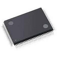
A54SX08A-TQG100 Actel, A54SX08A-TQG100 Datasheet - Page 15

A54SX08A-TQG100
Manufacturer Part Number
A54SX08A-TQG100
Description
FPGA - Field Programmable Gate Array 12K System Gates
Manufacturer
Actel
Datasheet
1.A54SX08A-TQG100.pdf
(108 pages)
Specifications of A54SX08A-TQG100
Processor Series
A54SX08
Core
IP Core
Number Of Macrocells
512
Maximum Operating Frequency
350 MHz
Number Of Programmable I/os
130
Delay Time
4 ns to 8.4 ns
Supply Voltage (max)
5.25 V
Maximum Operating Temperature
+ 70 C
Minimum Operating Temperature
0 C
Development Tools By Supplier
Silicon-Explorer II, Silicon-Sculptor 3, SI-EX-TCA
Mounting Style
SMD/SMT
Supply Voltage (min)
2.25 V
Number Of Gates
8000
Package / Case
TQFP-100
Lead Free Status / RoHS Status
Lead free / RoHS Compliant
Available stocks
Company
Part Number
Manufacturer
Quantity
Price
Company:
Part Number:
A54SX08A-TQG100
Manufacturer:
Microsemi SoC
Quantity:
10 000
Part Number:
A54SX08A-TQG100
Manufacturer:
MICROSEMI/美高森美
Quantity:
20 000
Company:
Part Number:
A54SX08A-TQG100A
Manufacturer:
Microsemi SoC
Quantity:
10 000
Company:
Part Number:
A54SX08A-TQG100I
Manufacturer:
Microsemi SoC
Quantity:
10 000
Probing Capabilities
SX-A devices also provide an internal probing capability
that is accessed with the JTAG pins. The Silicon Explorer II
diagnostic hardware is used to control the TDI, TCK, TMS,
and TDO pins to select the desired nets for debugging.
The user assigns the selected internal nets in Actel Silicon
Explorer II software to the PRA/PRB output pins for
observation. Silicon Explorer II automatically places the
device into JTAG mode. However, probing functionality is
only activated when the TRST pin is driven high or left
floating, allowing the internal pull-up resistor to pull
TRST High. If the TRST pin is held Low, the TAP controller
remains in the Test-Logic-Reset state so no probing can
be performed. However, the user must drive the TRST pin
High or allow the internal pull-up resistor to pull TRST
High.
Table 1-9 • Device Configuration Options for Probe Capability (TRST Pin Reserved)
JTAG Mode
Dedicated
Flexible
Notes:
1. If the TRST pin is not reserved, the device behaves according to TRST = High as described in the table.
2. Avoid using the TDI, TCK, TDO, PRA, and PRB pins as input or bidirectional ports. Since these pins are active during probing, input
3. If no user signal is assigned to these pins, they will behave as unused I/Os in this mode. Unused pins are automatically tristated by
signals will not pass through these pins and may cause contention.
the Designer software.
TRST
High
High
Low
Low
1
Security Fuse Programmed
Yes
No
No
No
No
v5.3
When selecting the Reserve Probe Pin box as shown in
Figure 1-12 on page
the PRA and PRB pins as dedicated outputs for probing.
This Reserve option is merely a guideline. If the designer
assigns user I/Os to the PRA and PRB pins and selects the
Reserve Probe Pin option, Designer Layout will
override the Reserve Probe Pin option and place the
user I/Os on those pins.
To allow probing capabilities, the security fuse must not
be programmed. Programming the security fuse disables
the JTAG and probe circuitry.
possible device configurations for probing once the
device leaves the Test-Logic-Reset JTAG state.
Probe Circuit Outputs
Probe Circuit Outputs
Probe Circuit Secured
PRA, PRB
User I/O
User I/O
1-9, direct the layout tool to reserve
3
3
2
Table 1-9
Probe Circuit Secured
TDI, TCK, TDO
SX-A Family FPGAs
JTAG Disabled
summarizes the
User I/O
JTAG I/O
JTAG I/O
3
2
1-11


