74LVC1T45GF,132 NXP Semiconductors, 74LVC1T45GF,132 Datasheet
74LVC1T45GF,132
Specifications of 74LVC1T45GF,132


Related parts for 74LVC1T45GF,132


74LVC1T45GF,132 Summary of contents
Page 1
Dual supply translating transceiver; 3-state Rev. 3 — 19 August 2010 1. General description The 74LVC1T45; 74LVCH1T45 are single bit, dual supply transceivers with 3-state outputs that enables bidirectional level translation. They feature one data input-output port (A ...
Page 2
... NXP Semiconductors Latch-up performance exceeds 100 mA per JESD 78 Class II ±24 mA output drive (V Inputs accept voltages up to 5.5 V Low power consumption: 16 μA maximum I I OFF Multiple package options Specified from −40 °C to +85 °C and −40 °C to +125 °C 3. Ordering information Table 1. ...
Page 3
... NXP Semiconductors 5. Functional diagram 5 DIR CC(A) Fig 1. Logic symbol 6. Pinning information 6.1 Pinning 74LVC1T45 74LVCH1T45 CC(A) CC(B) GND 2 5 DIR 001aaj991 Fig 3. Pin configuration SOT363 (SC-88) 6.2 Pin description Table 3. Pin description Symbol Pin V 1 CC(A) GND DIR CC(B) 74LVC_LVCH1T45 Product data sheet 74LVC1T45 ...
Page 4
... NXP Semiconductors 7. Functional description [1] Table 4. Function table Supply voltage Input DIR CC(A) CC( [3] GND X [ HIGH voltage level LOW voltage level don’t care high-impedance OFF-state. [2] The input circuit of the data I/O is always active. [3] When either GND level, the device goes into suspend mode. ...
Page 5
... NXP Semiconductors Table 6. Recommended operating conditions Symbol Parameter V output voltage O T ambient temperature amb Δt/ΔV input transition rise and fall rate [ the supply voltage associated with the output port. CCO [ the supply voltage associated with the input port. CCI 10. Static characteristics Table 7 ...
Page 6
... NXP Semiconductors Table 8. Static characteristics At recommended operating conditions; voltages are referenced to GND (ground = 0 V). Symbol Parameter Conditions V HIGH-level data input IH input voltage V CCI V CCI V CCI V CCI V CCI DIR input V CCI V CCI V CCI V CCI V CCI V LOW-level data input IL input voltage V CCI V CCI ...
Page 7
... NXP Semiconductors Table 8. Static characteristics At recommended operating conditions; voltages are referenced to GND (ground = 0 V). Symbol Parameter Conditions V LOW-level output voltage = 100 μ CCO input leakage DIR input current 5.5 V CCI I bus hold LOW port BHL current ...
Page 8
... NXP Semiconductors Table 8. Static characteristics At recommended operating conditions; voltages are referenced to GND (ground = 0 V). Symbol Parameter Conditions I power-off A port; V OFF leakage V CC(A) current V CC(B) B port CC(B) V CC(A) I supply current A port CC(A) V CC(A) V CC(A) V CC(A) B port CC(A) V CC(A) V CC(B) V CC(B) A plus B port ( ...
Page 9
... NXP Semiconductors 11. Dynamic characteristics Table 9. Typical dynamic characteristics at V Voltages are referenced to GND (ground = 0 V); for test circuit see Symbol Parameter t LOW to HIGH PLH propagation delay t HIGH to LOW PHL propagation delay t HIGH to OFF-state PHZ propagation delay t LOW to OFF-state PLZ propagation delay ...
Page 10
... NXP Semiconductors Table 11. Typical power dissipation capacitance at V Voltages are referenced to GND (ground = 0 V). Symbol Parameter Conditions C power dissipation A port: (direction A to B); PD capacitance B port: (direction port: (direction B to A); B port: (direction [ used to determine the dynamic power dissipation (P PD × V × f × ...
Page 11
... NXP Semiconductors Dynamic characteristics for temperature range −40 °C to +85 °C Table 12. Voltages are referenced to GND (ground = 0 V); for test circuit see Symbol Parameter Conditions t OFF-state to HIGH DIR to A PZH propagation delay DIR OFF-state to LOW DIR to A PZL propagation delay DIR ...
Page 12
... NXP Semiconductors Dynamic characteristics for temperature range −40 °C to +85 °C Table 12. Voltages are referenced to GND (ground = 0 V); for test circuit see Symbol Parameter Conditions t LOW to OFF-state DIR to A PLZ propagation delay DIR OFF-state to HIGH DIR to A PZH propagation delay DIR to B ...
Page 13
... NXP Semiconductors Dynamic characteristics for temperature range −40 °C to +125 °C Table 13. Voltages are referenced to GND (ground = 0 V); for test circuit see Symbol Parameter Conditions t OFF-state to LOW DIR to A PZL propagation delay DIR 2 2.7 V CC(A) t LOW to HIGH PLH propagation delay HIGH to LOW ...
Page 14
... NXP Semiconductors Dynamic characteristics for temperature range −40 °C to +125 °C Table 13. Voltages are referenced to GND (ground = 0 V); for test circuit see Symbol Parameter Conditions t OFF-state to HIGH DIR to A PZH propagation delay DIR OFF-state to LOW DIR to A PZL propagation delay DIR to B ...
Page 15
... NXP Semiconductors Table 14. Measurement points Supply voltage Input CC(A) CC( 1.6 V 0.5V 1. 2.7 V 0.5V 3 5.5 V 0.5V [ the supply voltage associated with the data input port. CCI [ the supply voltage associated with the output port. CCO Test data is given in Table R = Load resistance. ...
Page 16
... NXP Semiconductors 13. Typical propagation delay characteristics 14 t PHL (ns HIGH to LOW propagation delay ( PHL (ns HIGH to LOW propagation delay ( ( 1.2 V. CC(B) ( 1.5 V. CC(B) ( 1.8 V. CC(B) ( 2.5 V. CC(B) ( 3.3 V. CC(B) ( 5.0 V. CC(B) Fig 9. Typical propagation delay vs load capacitance; T 74LVC_LVCH1T45 Product data sheet 74LVC1T45; 74LVCH1T45 ...
Page 17
... NXP Semiconductors 14 t PHL (ns HIGH to LOW propagation delay ( PHL (ns HIGH to LOW propagation delay ( ( 1.2 V. CC(B) ( 1.5 V. CC(B) ( 1.8 V. CC(B) ( 2.5 V. CC(B) ( 3.3 V. CC(B) ( 5.0 V. CC(B) Fig 10. Typical propagation delay vs load capacitance; T 74LVC_LVCH1T45 Product data sheet 74LVC1T45; 74LVCH1T45 001aai911 14 t PLH (ns) ...
Page 18
... NXP Semiconductors 14 t PHL (ns HIGH to LOW propagation delay ( PHL (ns HIGH to LOW propagation delay ( ( 1.2 V. CC(B) ( 1.5 V. CC(B) ( 1.8 V. CC(B) ( 2.5 V. CC(B) ( 3.3 V. CC(B) ( 5.0 V. CC(B) Fig 11. Typical propagation delay vs load capacitance; T 74LVC_LVCH1T45 Product data sheet 74LVC1T45; 74LVCH1T45 001aai915 14 t PLH (ns) ...
Page 19
... NXP Semiconductors 14 t PHL (ns HIGH to LOW propagation delay ( PHL (ns HIGH to LOW propagation delay ( ( 1.2 V. CC(B) ( 1.5 V. CC(B) ( 1.8 V. CC(B) ( 2.5 V. CC(B) ( 3.3 V. CC(B) ( 5.0 V. CC(B) Fig 12. Typical propagation delay vs load capacitance; T 74LVC_LVCH1T45 Product data sheet 74LVC1T45; 74LVCH1T45 001aai919 14 t PLH (ns) ...
Page 20
... NXP Semiconductors 14 t PHL (ns HIGH to LOW propagation delay ( PHL (ns HIGH to LOW propagation delay ( ( 1.2 V. CC(B) ( 1.5 V. CC(B) ( 1.8 V. CC(B) ( 2.5 V. CC(B) ( 3.3 V. CC(B) ( 5.0 V. CC(B) Fig 13. Typical propagation delay vs load capacitance; T 74LVC_LVCH1T45 Product data sheet 74LVC1T45; 74LVCH1T45 001aai923 14 t PLH (ns) ...
Page 21
... NXP Semiconductors 14 t PHL (ns HIGH to LOW propagation delay ( PHL (ns HIGH to LOW propagation delay ( ( 1.2 V. CC(B) ( 1.5 V. CC(B) ( 1.8 V. CC(B) ( 2.5 V. CC(B) ( 3.3 V. CC(B) ( 5.0 V. CC(B) Fig 14. Typical propagation delay vs load capacitance; T 74LVC_LVCH1T45 Product data sheet 74LVC1T45; 74LVCH1T45 001aai927 14 t PLH (ns) ...
Page 22
... NXP Semiconductors 14. Application information 14.1 Unidirectional logic level-shifting application The circuit given unidirectional logic level-shifting application. Fig 15. Unidirectional logic level-shifting application Table 16. Pin 74LVC_LVCH1T45 Product data sheet 74LVC1T45; 74LVCH1T45 Figure example of the 74LVC1T45; 74LVCH1T45 being used V CC1 V CC(A) 1 GND V 2 CC1 ...
Page 23
... NXP Semiconductors 14.2 Bidirectional logic level-shifting application Figure 16 level-shifting application. Since the device does not have an output enable pin, the system designer should take precautions to avoid bus contention between system-1 and system-2 when changing directions. V I/O-1 DIR CTRL Fig 16. Bidirectional logic level-shifting application Table 17 and then from system-2 to system-1 ...
Page 24
... NXP Semiconductors 14.3 Power-up considerations The device is designed such that no special power-up sequence is required other than GND being applied first. Table 18. V CC( 1.8 V 2.5 V 3.3 V 5.0 V 14.4 Enable times Calculate the enable times for the 74LVC1T45; 74LVCH1T45 using the following formulas: • ...
Page 25
... NXP Semiconductors 15. Package outline Plastic surface-mounted package; 6 leads y 6 pin 1 index DIMENSIONS (mm are the original dimensions UNIT max 1.1 0.30 0.25 mm 0.1 0.8 0.20 0.10 OUTLINE VERSION IEC SOT363 Fig 17. Package outline SOT363 (SC-88) 74LVC_LVCH1T45 Product data sheet 74LVC1T45; 74LVCH1T45 scale ...
Page 26
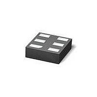
... NXP Semiconductors XSON6: plastic extremely thin small outline package; no leads; 6 terminals; body 1 x 1. 6× (2) terminal 1 index area DIMENSIONS (mm are the original dimensions) ( UNIT b D max max 0.25 1.5 mm 0.5 0.04 0.17 1.4 Notes 1. Including plating thickness. 2. Can be visible in some manufacturing processes. ...
Page 27
... NXP Semiconductors XSON6: plastic extremely thin small outline package; no leads; 6 terminals; body 0 6× (1) terminal 1 index area DIMENSIONS (mm are the original dimensions UNIT b D max max 0.20 1.05 mm 0.5 0.04 0.12 0.95 Note 1. Can be visible in some manufacturing processes. OUTLINE VERSION IEC SOT891 Fig 19 ...
Page 28
... NXP Semiconductors XSON6: extremely thin small outline package; no leads; 6 terminals; body 0.9 x 1 (6×) terminal 1 index area Dimensions (1) Unit max 0.35 0.04 0.20 0.95 mm nom 0.15 0.90 min 0.12 0.85 Note 1. Including plating thickness. 2. Visible depending upon used manufacturing technology. ...
Page 29
... NXP Semiconductors XSON6: extremely thin small outline package; no leads; 6 terminals; body 1.0 x 1 (6×) terminal 1 index area Dimensions (1) Unit max 0.35 0.04 0.20 1.05 mm nom 0.15 1.00 min 0.12 0.95 Note 1. Including plating thickness. 2. Visible depending upon used manufacturing technology. ...
Page 30
... NXP Semiconductors 16. Abbreviations Table 19. Abbreviations Acronym Description CDM Charged Device Model DUT Device Under Test ESD ElectroStatic Discharge HBM Human Body Model 17. Revision history Table 20. Revision history Document ID Release date 74LVC_LVCH1T45 v.3 20100819 • Modifications: Added type number 74LVC1T45GN (SOT1115/XSON6 package). ...
Page 31
... In no event shall NXP Semiconductors be liable for any indirect, incidental, punitive, special or consequential damages (including - without limitation - lost profits, lost savings, business interruption, costs related to the removal or ...
Page 32
... NXP Semiconductors Export control — This document as well as the item(s) described herein may be subject to export control regulations. Export might require a prior authorization from national authorities. 19. Contact information For more information, please visit: For sales office addresses, please send an email to: 74LVC_LVCH1T45 Product data sheet 74LVC1T45 ...
Page 33
... NXP Semiconductors 20. Contents 1 General description . . . . . . . . . . . . . . . . . . . . . . 1 2 Features and benefits . . . . . . . . . . . . . . . . . . . . 1 3 Ordering information . . . . . . . . . . . . . . . . . . . . . 2 4 Marking . . . . . . . . . . . . . . . . . . . . . . . . . . . . . . . . 2 5 Functional diagram . . . . . . . . . . . . . . . . . . . . . . 3 6 Pinning information . . . . . . . . . . . . . . . . . . . . . . 3 6.1 Pinning . . . . . . . . . . . . . . . . . . . . . . . . . . . . . . . 3 6.2 Pin description . . . . . . . . . . . . . . . . . . . . . . . . . 3 7 Functional description . . . . . . . . . . . . . . . . . . . 4 8 Limiting values Recommended operating conditions Static characteristics Dynamic characteristics . . . . . . . . . . . . . . . . . . 9 12 Waveforms . . . . . . . . . . . . . . . . . . . . . . . . . . . . 14 13 Typical propagation delay characteristics ...