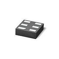
74LVC1T45GF,132 NXP Semiconductors, 74LVC1T45GF,132 Datasheet - Page 9

74LVC1T45GF,132
Manufacturer Part Number
74LVC1T45GF,132
Description
TXRX XLATING DUAL 3ST XSON6
Manufacturer
NXP Semiconductors
Datasheet
1.74LVCH1T45GW125.pdf
(33 pages)
Specifications of 74LVC1T45GF,132
Logic Family
74LVC
Number Of Channels Per Chip
2
Propagation Delay Time
29.5 ns
Supply Voltage (max)
5.5 V
Supply Voltage (min)
1.2 V
Maximum Operating Temperature
+ 125 C
Package / Case
XSON-6
Maximum Power Dissipation
250 mW
Minimum Operating Temperature
- 40 C
Mounting Style
SMD/SMT
Lead Free Status / RoHS Status
Lead free / RoHS Compliant
Other names
568-5459-2
NXP Semiconductors
11. Dynamic characteristics
Table 9.
Voltages are referenced to GND (ground = 0 V); for test circuit see
[1]
Table 10.
Voltages are referenced to GND (ground = 0 V); for test circuit see
[1]
74LVC_LVCH1T45
Product data sheet
Symbol Parameter
t
t
t
t
t
t
Symbol Parameter
t
t
t
t
t
t
PLH
PHL
PHZ
PLZ
PZH
PZL
PLH
PHL
PHZ
PLZ
PZH
PZL
t
t
PZH
PZH
and t
and t
LOW to HIGH
propagation delay
HIGH to LOW
propagation delay
HIGH to OFF-state
propagation delay
LOW to OFF-state
propagation delay
OFF-state to HIGH
propagation delay
OFF-state to LOW
propagation delay
LOW to HIGH
propagation delay
HIGH to LOW
propagation delay
HIGH to OFF-state
propagation delay
LOW to OFF-state
propagation delay
OFF-state to HIGH
propagation delay
OFF-state to LOW
propagation delay
Typical dynamic characteristics at V
Typical dynamic characteristics at V
PZL
PZL
are calculated values using the formula shown in
are calculated values using the formula shown in
Conditions
A to B
B to A
A to B
B to A
DIR to A
DIR to B
DIR to A
DIR to B
DIR to A
DIR to B
DIR to A
DIR to B
Conditions
A to B
B to A
A to B
B to A
DIR to A
DIR to B
DIR to A
DIR to B
DIR to A
DIR to B
DIR to A
DIR to B
All information provided in this document is subject to legal disclaimers.
Rev. 3 — 19 August 2010
CC(A)
CC(B)
[1]
[1]
[1]
[1]
[1]
[1]
[1]
[1]
= 1.2 V and T
= 1.2 V and T
1.2 V
1.2 V
10.6
10.6
10.1
10.1
12.0
20.1
17.7
22.1
19.5
10.6
10.6
10.1
10.1
12.0
20.1
17.7
22.1
19.5
Section 14.4 “Enable times”
Section 14.4 “Enable times”
9.4
7.1
9.5
9.4
7.1
9.5
74LVC1T45; 74LVCH1T45
Figure
Figure
1.5 V
1.5 V
amb
17.3
15.2
18.0
16.5
amb
15.4
14.4
13.2
15.1
8.1
9.5
7.1
8.6
9.4
9.4
7.1
7.8
9.5
8.1
8.6
7.1
6.5
6.1
4.9
7.3
Dual supply translating transceiver; 3-state
8; for waveforms see
8; for waveforms see
= 25 °C
= 25 °C
1.8 V
1.8 V
16.7
14.1
17.1
15.4
13.6
13.5
11.4
13.8
7.0
9.0
6.0
8.1
9.4
9.0
7.1
7.7
9.0
7.0
8.1
6.0
5.7
5.4
4.5
6.6
V
V
CC(B)
CC(A)
2.5 V
2.5 V
15.4
12.9
15.6
14.7
11.7
11.7
11.9
5.8
8.5
5.3
7.8
9.4
7.8
7.1
6.9
8.5
5.8
7.8
5.3
4.1
4.6
3.2
5.9
9.9
Figure 6
Figure 6
3.3 V
3.3 V
15.9
12.4
16.0
14.6
11.0
11.7
11.7
5.3
8.3
5.2
7.6
9.4
8.4
7.1
7.6
8.3
5.3
7.6
5.2
4.1
4.3
3.4
5.7
9.5
© NXP B.V. 2010. All rights reserved.
and
and
Figure 7
Figure 7
5.0 V
5.0 V
15.2
12.2
15.5
14.8
10.7
10.7
10.6
5.1
8.2
5.4
7.6
9.4
7.9
7.1
7.0
8.2
5.1
7.6
5.4
3.0
4.0
2.5
5.6
9.4
9 of 33
Unit
ns
ns
ns
ns
ns
ns
ns
ns
ns
ns
ns
ns
Unit
ns
ns
ns
ns
ns
ns
ns
ns
ns
ns
ns
ns


