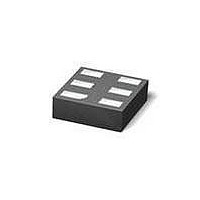
74LVC1T45GF,132 NXP Semiconductors, 74LVC1T45GF,132 Datasheet - Page 12

74LVC1T45GF,132
Manufacturer Part Number
74LVC1T45GF,132
Description
TXRX XLATING DUAL 3ST XSON6
Manufacturer
NXP Semiconductors
Datasheet
1.74LVCH1T45GW125.pdf
(33 pages)
Specifications of 74LVC1T45GF,132
Logic Family
74LVC
Number Of Channels Per Chip
2
Propagation Delay Time
29.5 ns
Supply Voltage (max)
5.5 V
Supply Voltage (min)
1.2 V
Maximum Operating Temperature
+ 125 C
Package / Case
XSON-6
Maximum Power Dissipation
250 mW
Minimum Operating Temperature
- 40 C
Mounting Style
SMD/SMT
Lead Free Status / RoHS Status
Lead free / RoHS Compliant
Other names
568-5459-2
NXP Semiconductors
Table 12.
Voltages are referenced to GND (ground = 0 V); for test circuit see
[1]
Table 13.
Voltages are referenced to GND (ground = 0 V); for test circuit see
74LVC_LVCH1T45
Product data sheet
Symbol Parameter
t
t
t
Symbol Parameter
V
t
t
t
t
t
t
V
t
t
t
t
t
PLZ
PZH
PZL
PLH
PHL
PHZ
PLZ
PZH
PZL
PLH
PHL
PHZ
PLZ
PZH
CC(A)
CC(A)
t
PZH
= 1.4 V to 1.6 V
= 1.65 V to 1.95 V
and t
LOW to OFF-state
propagation delay
OFF-state to HIGH
propagation delay
OFF-state to LOW
propagation delay
LOW to HIGH
propagation delay
HIGH to LOW
propagation delay
HIGH to OFF-state
propagation delay
LOW to OFF-state
propagation delay
OFF-state to HIGH
propagation delay
OFF-state to LOW
propagation delay
LOW to HIGH
propagation delay
HIGH to LOW
propagation delay
HIGH to OFF-state
propagation delay
LOW to OFF-state
propagation delay
OFF-state to HIGH
propagation delay
Dynamic characteristics for temperature range −40 °C to +85 °C
Dynamic characteristics for temperature range −40 °C to +125 °C
PZL
are calculated values using the formula shown in
Conditions
DIR to A
DIR to B
DIR to A
DIR to B
DIR to A
DIR to B
Conditions
A to B
B to A
A to B
B to A
DIR to A
DIR to B
DIR to A
DIR to B
DIR to A
DIR to B
DIR to A
DIR to B
A to B
B to A
A to B
B to A
DIR to A
DIR to B
DIR to A
DIR to B
DIR to A
DIR to B
[1]
[1]
[1]
[1]
[1]
[1]
[1]
[1]
[1]
[1]
All information provided in this document is subject to legal disclaimers.
1.5 V ± 0.1 V 1.8 V ± 0.15 V 2.5 V ± 0.2 V 3.3 V ± 0.3 V 5.0 V ± 0.5 V
1.5 V ± 0.1 V 1.8 V ± 0.15 V 2.5 V ± 0.2 V 3.3 V ± 0.3 V 5.0 V ± 0.5 V
Min
Min
1.4
2.3
2.5
2.5
2.3
2.3
2.7
3.1
2.1
2.5
2.3
2.1
2.1
1.9
2.6
2.8
2.1
2.2
-
-
-
-
-
-
-
-
-
-
Rev. 3 — 19 August 2010
Max
13.1
23.6
20.3
28.1
20.7
Max
23.5
23.5
21.3
21.3
20.6
27.3
12.6
20.2
43.7
36.1
48.6
41.9
21.1
19.4
19.1
16.9
18.9
26.6
19.4
38.8
32.7
11.6
3.7
Section 14.4 “Enable times”
Min
Min
1.4
2.4
2.1
2.3
1.9
2.1
2.7
3.1
2.1
2.7
1.9
1.9
1.8
1.8
2.6
2.8
2.1
2.3
-
-
-
-
-
-
-
-
-
-
74LVC1T45; 74LVCH1T45
Figure
Figure
Max
12.1
18.9
18.8
23.1
17.6
Max
19.4
21.1
16.9
19.1
20.6
26.0
12.6
19.0
40.1
32.0
45.1
37.5
19.5
19.5
15.8
15.8
18.9
24.1
11.6
17.6
37.1
31.1
3.7
Dual supply translating transceiver; 3-state
8; for wave forms see
8; for wave forms see
Min
Min
1.3
1.9
1.8
2.0
1.6
2.0
2.7
2.7
2.1
2.2
1.9
2.0
1.4
1.8
2.6
2.4
2.1
1.9
-
-
-
-
V
-
-
-
-
-
-
V
CC(B)
CC(B)
…continued
Max
12.2
14.3
11.2
11.6
Max
14.9
16.4
13.0
14.6
20.6
12.1
12.6
10.4
26.8
27.5
26.7
33.6
10.3
17.6
14.2
18.9
12.7
10.2
27.8
21.9
11.6
3.7
7.4
9.4
Min
1.0
2.3
Min
1.5
2.0
1.5
1.9
2.7
2.9
2.1
2.7
1.5
1.8
1.6
1.8
2.6
2.7
2.1
2.4
-
-
-
-
-
-
-
-
-
-
Figure 6
Figure 6
Max
11.4
12.0
Max
13.0
13.7
12.0
12.5
20.6
12.5
12.6
24.9
25.6
25.0
32.6
17.1
13.9
18.9
26.4
19.6
11.2
11.4
11.6
3.7
7.0
9.1
9.9
8.0
7.9
9.3
© NXP B.V. 2010. All rights reserved.
and
and
Min
0.9
1.8
Min
1.4
1.9
1.5
2.0
2.7
2.5
2.1
2.2
1.2
1.7
1.5
1.6
2.6
2.2
2.1
2.1
-
-
-
-
-
-
-
-
-
-
Figure 7
Figure 7
Max
Max
13.2 ns
12.1 ns
20.6 ns
12.6 ns
10.4 ns
23.6 ns
24.2 ns
23.5 ns
32.5 ns
16.7 ns
13.5 ns
18.9 ns
24.1 ns
19.1 ns
11.6 ns
11.9 ns
11.4 ns
11.6 ns
3.7
4.5
8.4
7.6
9.2
8.9
7.5
7.7
9.1
7.4
12 of 33
Unit
ns
ns
ns
ns
ns
ns
Unit
ns
ns
ns
ns


