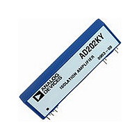
AD204JN Analog Devices Inc, AD204JN Datasheet - Page 4

AD204JN
Manufacturer Part Number
AD204JN
Description
IC, ISOLATION AMPLIFIER, 5KHZ, DIP-10
Manufacturer
Analog Devices Inc
Type
Isolation Amplifierr
Datasheet
1.AD202JN.pdf
(12 pages)
Specifications of AD204JN
No. Of Amplifiers
1
Isolation Voltage
750Vrms
Gain Non-linearity Max
0.05%
Amplifier Case Style
DIP
No. Of Pins
10
Input Offset Voltage
15mV
Bandwidth
5kHz
Rohs Status
RoHS non-compliant
Amplifier Type
Isolation
Number Of Circuits
4
Gain Bandwidth Product
5kHz
Current - Input Bias
30pA
Voltage - Input Offset
15000µV
Current - Output / Channel
2mA
Operating Temperature
0°C ~ 70°C
Mounting Type
Through Hole
Package / Case
38-DIP (0.500", 12.70mm), 11 Leads
Number Of Channels
1
Number Of Elements
1
Common Mode Rejection Ratio
130dB
Voltage Gain Db
40dB
Input Resistance
2000MOhm
Input Bias Current
30pA
Rail/rail I/o Type
No
Operating Temp Range
-40C to 85C
Operating Temperature Classification
Industrial
Mounting
Through Hole
Pin Count
11
Package Type
PDIP
Lead Free Status / RoHS Status
Contains lead / RoHS non-compliant
Current - Supply
-
Output Type
-
Voltage - Supply, Single/dual (±)
-
-3db Bandwidth
-
Slew Rate
-
Lead Free Status / Rohs Status
Not Compliant
AD202/AD204
DIFFERENCES BETWEEN THE AD202 AND AD204
The primary distinction between the AD202 and AD204 is in
the method by which they are powered: the AD202 operates
directly from 15 V dc while the AD204 is powered by a non-
isolated externally-supplied clock (AD246) that can drive up to
32 AD204s. The main advantages of using the externally-
clocked AD204 over the AD202 are reduced cost in multichannel
applications, lower power consumption, and higher bandwidth.
In addition, the AD204 can supply substantially more isolated
power than the AD202.
Of course, in a great many situations, especially where only one
or a few isolators are used, the convenience of standalone opera-
tion provided by the AD202 will be more significant than any
of the AD204’s advantages. There may also be cases where it is
desirable to accommodate either device interchangeably, so the
pinouts of the two products have been designed to make that
easy to do.
INSIDE THE AD202 AND AD204
The AD202 and AD204 use an amplitude modulation technique
to permit transformer coupling of signals down to dc (Figure 1a
and 1b). Both models also contain an uncommitted input op
amp and a power transformer that provides isolated power to
the op amp, the modulator, and any external load. The power
transformer primary is driven by a 25 kHz, 15 V p-p square
wave generated internally in the case of the AD202, or supplied
externally for the AD204.
Within the signal swing limits of approximately ± 5 V, the out-
put voltage of the isolator is equal to the output voltage of the
op amp; that is, the isolation barrier has unity gain. The output
signal is not internally buffered, so the user is free to interchange
V
+V
–V
V
+V
–V
Figure 1b. AD204 Functional Block Diagram
(Pin Designations Apply to the DIP-Style Package)
SIG
SIG
ISO
ISO
ISO
ISO
IN COM
IN COM
OUT
OUT
OUT
OUT
IN–
IN+
IN–
IN+
FB
FB
Figure 1a. AD202 Functional Block Diagram
+7.5V
+7.5V
–7.5V
–7.5V
FS
FS
5V
5V
FILTER
FILTER
RECT
RECT
AND
AND
MOD
MOD
25kHz
25kHz
POWER
POWER
SIGNAL
SIGNAL
25kHz
25kHz
DEMOD
DEMOD
OSCILLATOR
POWER
CONV.
AD204
AD202
FS
FS
5V
5V
HI
LO
CLOCK
15V p-p
25kHz
POWER
RETURN
POWER
RETURN
HI
LO
15V DC
V
V
OUT
OUT
–4–
the output leads to get signal inversion. Additionally, in multi-
channel applications, the unbuffered outputs can be multiplexed
with one buffer following the mux. This technique minimizes
offset errors while reducing power consumption and cost. The
output resistance of the isolator is typically 3 kΩ for the AD204
(7 kΩ for AD202) and varies with signal level and temperature,
so it should not be loaded (see Figure 2 for the effects of load
upon nonlinearity and gain drift). In many cases, a high imped-
ance load will be present or a following circuit such as an output
filter can serve as a buffer so that a separate buffer function will
not often be needed.
USING THE AD202 AND AD204
Powering the AD202. The AD202 requires only a single 15 V
power supply connected as shown in Figure 3a. A bypass capaci-
tor is provided in the module.
Powering the AD204. The AD204 gets its power from an
externally supplied clock signal (a 15 V p-p square wave with a
nominal frequency of 25 kHz) as shown in Figure 3b.
(NOTE: Circuit figures shown on this page are for SIP-style packages. Refer to
Page 3 for proper DIP package pinout.)
LINEARITY
NON-
0.25
0.20
0.15
0.10
0.05
(%)
0
0
AD204 NONLINEARITY
AD204
0.1
Figure 2. Effects of Output Loading
0.2
AD202 GAIN AND GAIN TC
AD202 NONLINEARITY
AD204 GAIN AND GAIN TC
AD204
0.3
OUTPUT LOAD – M
0.4
AD202
Figure 3a.
AD204
Figure 3b.
0.5
15V RETURN
0.6
15V
AD246
5%
0.7
0.8
+
0.9
15V RETURN
15V
CHANGE
1.0
GAIN
(%)
–10
–8
–6
–4
–2
0
REV. D
CHANGE
GAIN TC
(ppm/ C)
–500
–400
–300
–200
–100
0


