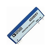
AD204JN Analog Devices Inc, AD204JN Datasheet - Page 6

AD204JN
Manufacturer Part Number
AD204JN
Description
IC, ISOLATION AMPLIFIER, 5KHZ, DIP-10
Manufacturer
Analog Devices Inc
Type
Isolation Amplifierr
Datasheet
1.AD202JN.pdf
(12 pages)
Specifications of AD204JN
No. Of Amplifiers
1
Isolation Voltage
750Vrms
Gain Non-linearity Max
0.05%
Amplifier Case Style
DIP
No. Of Pins
10
Input Offset Voltage
15mV
Bandwidth
5kHz
Rohs Status
RoHS non-compliant
Amplifier Type
Isolation
Number Of Circuits
4
Gain Bandwidth Product
5kHz
Current - Input Bias
30pA
Voltage - Input Offset
15000µV
Current - Output / Channel
2mA
Operating Temperature
0°C ~ 70°C
Mounting Type
Through Hole
Package / Case
38-DIP (0.500", 12.70mm), 11 Leads
Number Of Channels
1
Number Of Elements
1
Common Mode Rejection Ratio
130dB
Voltage Gain Db
40dB
Input Resistance
2000MOhm
Input Bias Current
30pA
Rail/rail I/o Type
No
Operating Temp Range
-40C to 85C
Operating Temperature Classification
Industrial
Mounting
Through Hole
Pin Count
11
Package Type
PDIP
Lead Free Status / RoHS Status
Contains lead / RoHS non-compliant
Current - Supply
-
Output Type
-
Voltage - Supply, Single/dual (±)
-
-3db Bandwidth
-
Slew Rate
-
Lead Free Status / Rohs Status
Not Compliant
AD202/AD204
Adjustments. When gain and zero adjustments are needed, the
circuit details will depend on whether adjustments are to be made
at the isolator input or output, and (for input adjustments) on
the input circuit used. Adjustments are usually best done on the
input side, because it is better to null the zero ahead of the gain,
and because gain adjustment is most easily done as part of the
gain-setting network. Input adjustments are also to be preferred
when the pots will be near the input end of the isolator (to mini-
mize common-mode strays). Adjustments on the output side
might be used if pots on the input side would represent a hazard
due to the presence of large common-mode voltages during
adjustment.
Figure 8a shows the input-side adjustment connections for use
with the noninverting connection of the input amplifier. The
zero adjustment circuit injects a small adjustment voltage in series
with the low side of the signal source. (This will not work if the
source has another current path to input common or if current
flows in the signal source LO lead). Since the adjustment volt-
age is injected ahead of the gain, the values shown will work for
any gain. Keep the resistance in series with input LO below a
few hundred ohms to avoid CMR degradation.
Also shown in Figure 8a is the preferred means of adjusting the
gain-setting network. The circuit shown gives a nominal R
50 kW, and will work properly for gains of ten or greater. The
adjustment becomes less effective at lower gains (its effect is
halved at G = 2) so that the pot will have to be a larger fraction
of the total R
be adjusted downward without compromising input resistance;
it is better to adjust gain at the signal source or after the output.
Figure 8b shows adjustments for use with inverting input cir-
cuits. The zero adjustment nulls the voltage at the summing
node. This method is preferable to current injection because it is
less affected by subsequent gain adjustment. Gain adjustment is
again done in the feedback; but in this case it will work all the
way down to unity gain (and below) without alteration.
(NOTE: Circuit figures shown on this page are for SIP-style packages. Refer to
Page 3 for proper DIP package pinout.)
Figure 8a. Adjustments for Noninverting Connection of
Op Amp
V
S
47.5k
200
F
at low gain. At G = 1 (follower) the gain cannot
R
G
50k
GAIN
5k
100k
ZERO
2k
+7.5
–7.5
AD202
AD204
OR
F
of
–6–
Figure 9 shows how zero adjustment is done at the output by
taking advantage of the semi-floating output port. The range of
this adjustment will have to be increased at higher gains; if that
is done, be sure to use a suitably stable supply voltage for the
pot circuit.
There is no easy way to adjust gain at the output side of the
isolator itself. If gain adjustment must be done on the output
side, it will have to be in a following circuit such as an output
buffer or filter.
Common-Mode Performance. Figures 10a and 10b show
how the common-mode rejection of the AD202 and AD204
varies with frequency, gain, and source resistance. For these
isolators, the significant resistance will normally be that in the
path from the source of the common-mode signal to IN COM.
The AD202 and AD204 also perform well in applications re-
quiring rejection of fast common-mode steps, as described in
the Applications section.
Figure 8b. Adjustments for Summing or Current Input
V
180
160
140
120
100
S
80
60
40
Figure 9. Output-Side Zero Adjustment
10
R
50k
20
S
GAIN
47.5k
5k
100k
Figure 10a. AD204
200
50 60 100
ZERO
AD202
AD204
OR
FREQUENCY – Hz
200
200
+7.5
–7.5
500
V
O
0.1 F
50k
1k
AD202
AD204
+15V
–15V
OR
2k
G = 100
G = 1
100k
ZERO
REV. D
5k


