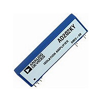
AD204JN Analog Devices Inc, AD204JN Datasheet - Page 9

AD204JN
Manufacturer Part Number
AD204JN
Description
IC, ISOLATION AMPLIFIER, 5KHZ, DIP-10
Manufacturer
Analog Devices Inc
Type
Isolation Amplifierr
Datasheet
1.AD202JN.pdf
(12 pages)
Specifications of AD204JN
No. Of Amplifiers
1
Isolation Voltage
750Vrms
Gain Non-linearity Max
0.05%
Amplifier Case Style
DIP
No. Of Pins
10
Input Offset Voltage
15mV
Bandwidth
5kHz
Rohs Status
RoHS non-compliant
Amplifier Type
Isolation
Number Of Circuits
4
Gain Bandwidth Product
5kHz
Current - Input Bias
30pA
Voltage - Input Offset
15000µV
Current - Output / Channel
2mA
Operating Temperature
0°C ~ 70°C
Mounting Type
Through Hole
Package / Case
38-DIP (0.500", 12.70mm), 11 Leads
Number Of Channels
1
Number Of Elements
1
Common Mode Rejection Ratio
130dB
Voltage Gain Db
40dB
Input Resistance
2000MOhm
Input Bias Current
30pA
Rail/rail I/o Type
No
Operating Temp Range
-40C to 85C
Operating Temperature Classification
Industrial
Mounting
Through Hole
Pin Count
11
Package Type
PDIP
Lead Free Status / RoHS Status
Contains lead / RoHS non-compliant
Current - Supply
-
Output Type
-
Voltage - Supply, Single/dual (±)
-
-3db Bandwidth
-
Slew Rate
-
Lead Free Status / Rohs Status
Not Compliant
Synchronization. Since AD204s operate from a common
clock, synchronization is inherent. AD202s will normally not
interact to produce beat frequencies even when mounted on
0.25-inch centers. Interaction may occur in rare situations where
a large number of long, unshielded input cables are bundled
together and channel gains are high. In such cases, shielded
cable may be required or AD204s can be used.
APPLICATIONS EXAMPLES
Low Level Sensor Inputs. In applications where the output of
low level sensors such as thermocouples must be isolated, a low
drift input amplifier can be used with an AD204, as shown in
REV. D
GRID
0.1”
100pF
1
3
5
R
CHANNEL 0
F
HI
LO
HI
Figure 16b.
LO
R
39k
G
2
4
6
1
3
5
R
CHANNEL 1
F
+
OPEN INPUT
DETECTION
HI
OPTIONAL
Figure 17. Input Amplifier and Filter for Sensor Signals
220M
1 F
LO
R
G
2
4
6
AD OP-07
100pF
49.9k
R
470k
1 F
G
0.038 F
+
0.15 F
–9–
470k
1 F
Figure 17. A three-pole active filter is included in the design to
get normal-mode rejection of frequencies above a few Hz and to
provide enhanced common-mode rejection at 60 Hz. If offset
adjustment is needed, it is best done at the trim pins of the OP07
itself; gain adjustment can be done at the feedback resistor.
Note that the isolated supply current is large enough to mandate
the use of 1 mF supply bypass capacitors. This circuit can be
used with an AD202 if a low power op amp is used instead of
the OP07.
Process Current Input with Offset. Figure 18 shows an
isolator receiver that translates a 4-20 mA process current
signal into a 0 V to 10 V output. A 1 V to 5 V signal appears at
the isolator’s output, and a –1 V reference applied to output LO
provides the necessary level shift (in multichannel applications,
the reference can be shared by all channels). This technique is
often useful for getting offset with a follower-type output buffer.
The circuit as shown requires a source compliance of at least
5 V, but if necessary that can be reduced by using a lower value
of current-sampling resistor and configuring the input amplifier
for a small gain.
(NOTE: Circuit figures shown on this page are for SIP-style packages. Refer to
Page 3 for proper DIP package pinout.)
4–20mA
+
Figure 18. Process Current Input Isolator with Offset
–7.5V
+7.5V
250
AD204
ADDITIONAL
CHANNELS
CLK
–1V TO
V
O
AD202
AD204
–
+
CLK RET
= V
OR
I
(
237
1 +
+
–
50k
1V
TO
5V
R
G
AD202/AD204
AD589
1k
)
–15V
6.8k
+15V
–15V
10k
15k
0V
TO
10V
+
–


