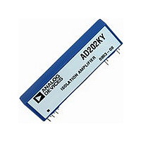
AD204JN Analog Devices Inc, AD204JN Datasheet - Page 7

AD204JN
Manufacturer Part Number
AD204JN
Description
IC, ISOLATION AMPLIFIER, 5KHZ, DIP-10
Manufacturer
Analog Devices Inc
Type
Isolation Amplifierr
Datasheet
1.AD202JN.pdf
(12 pages)
Specifications of AD204JN
No. Of Amplifiers
1
Isolation Voltage
750Vrms
Gain Non-linearity Max
0.05%
Amplifier Case Style
DIP
No. Of Pins
10
Input Offset Voltage
15mV
Bandwidth
5kHz
Rohs Status
RoHS non-compliant
Amplifier Type
Isolation
Number Of Circuits
4
Gain Bandwidth Product
5kHz
Current - Input Bias
30pA
Voltage - Input Offset
15000µV
Current - Output / Channel
2mA
Operating Temperature
0°C ~ 70°C
Mounting Type
Through Hole
Package / Case
38-DIP (0.500", 12.70mm), 11 Leads
Number Of Channels
1
Number Of Elements
1
Common Mode Rejection Ratio
130dB
Voltage Gain Db
40dB
Input Resistance
2000MOhm
Input Bias Current
30pA
Rail/rail I/o Type
No
Operating Temp Range
-40C to 85C
Operating Temperature Classification
Industrial
Mounting
Through Hole
Pin Count
11
Package Type
PDIP
Lead Free Status / RoHS Status
Contains lead / RoHS non-compliant
Current - Supply
-
Output Type
-
Voltage - Supply, Single/dual (±)
-
-3db Bandwidth
-
Slew Rate
-
Lead Free Status / Rohs Status
Not Compliant
Dynamics and Noise. Frequency response plots for the AD202
and AD204 are given in Figure 11. Since neither isolator is slew-
rate limited, the plots apply for both large and small signals.
Capacitive loads of up to 470 pF will not materially affect fre-
quency response. When large signals beyond a few hundred Hz
will be present, it is advisable to bypass –V
COM with 1 mF tantalum capacitors even if the isolated supplies
are not loaded.
At 50 Hz/60 Hz, phase shift through the AD202/AD204 is typically
0.8∞ (lagging). Typical unit to unit variation is ±0.2∞ (lagging).
The step response of the AD204 for very fast input signals can
be improved by the use of an input filter, as shown in Figure 12.
The filter limits the bandwidth of the input (to about 5.3 kHz)
so that the isolator does not see fast, out-of-band input terms
that can cause small amounts (± 0.3%) of internal ringing. The
AD204 will then settle to ± 0.1% in about 300 ms for a 10 V
step.
REV. D
Figure 12. Input Filter for Improved Step Response
–20
–40
Figure 11. Frequency Response at Several Gains
60
40
20
0
10
180
160
140
120
100
80
60
40
V
10
S
20
20
RESPONSE
AD204
AD202
50
3.3k
PHASE
(G = 1)
0.01 F
AMPLITUDE
RESPONSE
100
Figure 10b. AD202
50 60 100
FREQUENCY – Hz
200
FREQUENCY – Hz
500
200
1k
500
2k
ISO
1k
5k
and +V
AD204
10k 20k
G = 100
G = 1
2k
ISO
0
–50
–100
5k
to IN
–7–
Except at the highest useful gains, the noise seen at the output
of the AD202 and AD204 will be almost entirely comprised of
carrier ripple at multiples of 25 kHz. The ripple is typically
2 mV p-p near zero output and increases to about 7 mV p-p for
outputs of ± 5 V (1 MHz measurement bandwidth). Adding a
capacitor across the output will reduce ripple at the expense of
bandwidth: for example, 0.05 mF at the output of the AD204
will result in 1.5 mV ripple at ± 5 V, but signal bandwidth will
be down to 1 kHz.
When the full isolator bandwidth is needed, the simple two-pole
active filter shown in Figure 13 can be used. It will reduce ripple
to 0.1 mV p-p with no loss of signal bandwidth, and also serves
as an output buffer.
An output buffer or filter may sometimes show output spikes
that do not appear at its input. This is usually due to clock noise
appearing at the op amp’s supply pins (since most op amps have
little or no supply rejection at high frequencies). Another com-
mon source of carrier-related noise is the sharing of a ground
track by both the output circuit and the power input. Figure 13
shows how to avoid these problems: the clock/supply port of the
isolator does not share ground or 15 V tracks with any signal
circuits, and the op amp’s supply pins are bypassed to signal
common (note that the grounded filter capacitor goes here as
well). Ideally, the output signal LO lead and the supply com-
mon meet where the isolator output is actually measured, e.g.,
at an A/D converter input. If that point is more than a few feet
from the isolator, it may be useful to bypass output LO to sup-
ply common at the isolator with a 0.1 mF capacitor.
In applications where more than a few AD204s are driven by a
single clock driver, substantial current spikes will flow in the
power return line and in whichever signal out lead returns to a
low impedance point (usually output LO). Both of these tracks
should be made large to minimize inductance and resistance;
ideally, output LO should be directly connected to a ground
plane which serves as measurement common.
Current spikes can be greatly reduced by connecting a small
inductance (68 mH–100 mH) in series with the clock pin of each
AD204. Molded chokes such as the Dale IM-2 series, with dc
resistance of about 5 W, are suitable.
(NOTE: Circuit figures shown on this page are for SIP-style packages. Refer to
Page 3 for proper DIP package pinout.)
Figure 13. Output Filter Circuit Showing Proper Grounding
AD202
AD204
OR
10k
1000pF
(IF USED)
10k
2200pF
AD246
AD711
–15V
AD202/AD204
1.0 F 1.0 F
SUPPLY
POWER
+
C
+15V
+
MEASUREMENT
POINT OF


