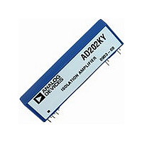
AD204JN Analog Devices Inc, AD204JN Datasheet - Page 5

AD204JN
Manufacturer Part Number
AD204JN
Description
IC, ISOLATION AMPLIFIER, 5KHZ, DIP-10
Manufacturer
Analog Devices Inc
Type
Isolation Amplifierr
Datasheet
1.AD202JN.pdf
(12 pages)
Specifications of AD204JN
No. Of Amplifiers
1
Isolation Voltage
750Vrms
Gain Non-linearity Max
0.05%
Amplifier Case Style
DIP
No. Of Pins
10
Input Offset Voltage
15mV
Bandwidth
5kHz
Rohs Status
RoHS non-compliant
Amplifier Type
Isolation
Number Of Circuits
4
Gain Bandwidth Product
5kHz
Current - Input Bias
30pA
Voltage - Input Offset
15000µV
Current - Output / Channel
2mA
Operating Temperature
0°C ~ 70°C
Mounting Type
Through Hole
Package / Case
38-DIP (0.500", 12.70mm), 11 Leads
Number Of Channels
1
Number Of Elements
1
Common Mode Rejection Ratio
130dB
Voltage Gain Db
40dB
Input Resistance
2000MOhm
Input Bias Current
30pA
Rail/rail I/o Type
No
Operating Temp Range
-40C to 85C
Operating Temperature Classification
Industrial
Mounting
Through Hole
Pin Count
11
Package Type
PDIP
Lead Free Status / RoHS Status
Contains lead / RoHS non-compliant
Current - Supply
-
Output Type
-
Voltage - Supply, Single/dual (±)
-
-3db Bandwidth
-
Slew Rate
-
Lead Free Status / Rohs Status
Not Compliant
AD246 Clock Driver. The AD246 is a compact, inexpensive
clock driver that can be used to obtain the required clock from a
single 15 V supply. Alternatively, the circuit shown in Figure 4
(essentially an AD246) can be used. In either case, one clock
circuit can operate at least 32 AD204s at the rated minimum
supply voltage of 14.25 V and one additional isolator can be
operated for each 40 mV increase in supply voltage up to 15 V.
A supply bypass capacitor is included in the AD246, but if many
AD204s are operated from a single AD246, an external bypass
capacitor should be used with a value of at least 1 mF for every
five isolators used. Place the capacitor as close as possible to the
clock driver.
Input Configurations. The AD202 and AD204 have been
designed to be very easy to use in a wide range of applications.
The basic connection for standard unity gain applications, useful
for signals up to ± 5 V, is shown in Figure 5; some of the possible
variations are described below. When smaller signals must be
handled, Figure 6 shows how to achieve gain while preserving a
very high input resistance. The value of feedback resistor R
should be kept above 20 kW for best results. Whenever a gain of
more than five is taken, a 100 pF capacitor from FB to IN COM
is required. At lower gains this capacitor is unnecessary, but it
will not adversely affect performance if used.
REV. D
49.9k
180pF
( 5V)
V
SIG
1
3
2
(SEE TEXT)
C
RC
R
Figure 5. Basic Unity-Gain Application
12 9
2k
14
4047B
CD
6
8
Figure 4. Clock Driver
7
5
Q
4
IN+
IN COM
FB
IN–
10
2
4
AD202
AD204
TELEDYNE
OR
TSC426
6
3
OUT
OUT
7
5
1N914
1N914
LO
HI
+ 1 F
35V
15V OR
CLOCK
15V
CLK
OUT
CLK AND
PWR COM
V
OUT
5V
F
–5–
The noninverting circuit of Figures 5 and 6 can also be used to
your advantage when a signal inversion is needed: just interchange
either the input leads or the output leads to get inversion. This
approach retains the high input resistance of the noninverting
circuit, and at unity gain no gain-setting resistors are needed.
When the isolator is not powered, a negative input voltage of
more than about 2 V will cause an input current to flow. If the
signal source can supply more than a few mA under such con-
ditions, the 2 kW resistor shown in series with IN+ should be
used to limit current to a safe value. This is particularly impor-
tant with the AD202, which may not start if a large input current
is present.
Figure 7 shows how to accommodate current inputs or sum
currents or voltages. This circuit can also be used when the
input signal is larger than the ± 5 V input range of the isolator;
for example, a ± 50 V input span can be accommodated with
R
to IN COM is required for gains above five.
(NOTE: Circuit figures shown on this page are for SIP-style packages. Refer to
Page 3 for proper DIP package pinout.)
V
F
Figure 7. Connections for Summing or Current Inputs
SIG
= 20 kW and R
V
S2
100pF
2k
Figure 6. Input Connections for Gain > 1
I
S
V = –
R
S2
V
R
S1
S1
S
(
R
R
V
= 200 kW. Once again, a capacitor from FB
F
G
S1
––– + V
R
R
S1
F
R
F
R
S2
F
20k
––– + I
R
R
S2
F
S
R
F
AD202
AD204
AD202/AD204
+ ...
OR
)
AD202
AD204
V
OR
O
V
= V
O
R
SIG
F
20k
(
1 + –––
V
R
R
G
F
)


