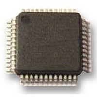
SC16C650BIB48 NXP Semiconductors, SC16C650BIB48 Datasheet - Page 24

SC16C650BIB48
Manufacturer Part Number
SC16C650BIB48
Description
UART, 32BYTE FIFO, 16C650, LQFP48
Manufacturer
NXP Semiconductors
Datasheet
1.SC16C650BIB48151.pdf
(48 pages)
Specifications of SC16C650BIB48
No. Of Channels
1
Data Rate
3Mbps
Supply Voltage Range
2.25V To 5.5V
Operating Temperature Range
-40°C To +85°C
Digital Ic Case Style
LQFP
No. Of Pins
48
Svhc
No SVHC (18-Jun-2010)
Operating
RoHS Compliant
Uart Features
Automatic Software/Hardware Flow Control, Programmable Xon/Xoff Characters
Rohs Compliant
Yes
Available stocks
Company
Part Number
Manufacturer
Quantity
Price
Company:
Part Number:
SC16C650BIB48,151
Manufacturer:
NXP Semiconductors
Quantity:
10 000
Company:
Part Number:
SC16C650BIB48151
Manufacturer:
NXP Semiconductors
Quantity:
135
NXP Semiconductors
SC16C650B_4
Product data sheet
Table 19.
Bit
5
4
3
2
1
0
Symbol
MCR[5]
MCR[4]
MCR[3]
MCR[2]
MCR[1]
MCR[0]
Modem Control Register bits description
Description
INT type select.
Loopback. Enable the local loopback mode (diagnostics). In this mode the
transmitter output (TX) and the receiver input (RX), CTS, DSR, DCD, and RI are
disconnected from the SC16C650B I/O pins. Internally the modem data and
control pins are connected into a loopback data configuration (see
this mode, the receiver and transmitter interrupts remain fully operational. The
Modem Control Interrupts are also operational, but the interrupts’ sources are
switched to the lower four bits of the Modem Control. Interrupts continue to be
controlled by the IER register.
OUT2. In the loopback mode this bit is used to control the modem DCD signal
via OUT2.
OUT1, OUT. In the loopback mode, this bit is used to control modem RI interface
signal via OUT1 (OUT in the HVQFN32 package).
RTS
DTR
logic 0 = enable interrupt output mode (normal default condition)
logic 1 = enable open source interrupt output mode. Provides shared
interrupts by producing a wire-OR output driver capability for interrupts. This
output appears at the INT pin. When using this option, an external pull-down
resistor of 200
an acceptable logic 0 level
logic 0 = disable loopback mode (normal default condition)
logic 1 = enable local loopback mode (diagnostics)
logic 0 = OUT2 is at logic 1. In the loopback mode, sets OUT2 (DCD)
internally to a logic 1.
logic 1 = OUT2 is at logic 0. In the loopback mode, sets OUT2 (DCD)
internally to a logic 0.
logic 0 = OUT1/OUT is at logic 1. In the loopback mode, sets RI internally to
logic 1.
logic 1 = OUT1/OUT is set at logic 0. In the loopback mode, sets RI internally
to logic 0.
logic 0 = force RTS output to a logic 1 (normal default condition)
logic 1 = force RTS output to a logic 0
logic 0 = force DTR output to a logic 1 (normal default condition)
logic 1 = force DTR output to a logic 0
Rev. 04 — 14 September 2009
UART with 32-byte FIFOs and IrDA encoder/decoder
to 500
must be tied from the INT pin to ground to provide
…continued
SC16C650B
© NXP B.V. 2009. All rights reserved.
Figure
7). In
24 of 48


