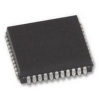
AT80C51RD2-SLSUM Atmel, AT80C51RD2-SLSUM Datasheet - Page 15

AT80C51RD2-SLSUM
Manufacturer Part Number
AT80C51RD2-SLSUM
Description
MCU, 8BIT, 8051, 5V, SPI, 20MHZ, 44PLCC
Manufacturer
Atmel
Specifications of AT80C51RD2-SLSUM
Controller Family/series
(8051) 8052
No. Of I/o's
32
Ram Memory Size
1280Byte
Cpu Speed
40MHz
No. Of Timers
3
No. Of Pwm Channels
5
Core Size
8bit
Oscillator Type
External Only
Processor Series
AT80x
Core
8051
Data Bus Width
8 bit
Program Memory Type
ROMLess
Data Ram Size
1280 B
Interface Type
UART, SPI
Maximum Clock Frequency
60 MHz
Number Of Programmable I/os
32
Number Of Timers
3
Operating Supply Voltage
2.7 V to 5.5 V
Maximum Operating Temperature
+ 85 C
Mounting Style
SMD/SMT
Package / Case
PLCC
3rd Party Development Tools
PK51, CA51, A51, ULINK2
Minimum Operating Temperature
- 40 C
Cpu Family
AT80
Device Core
8051
Device Core Size
8b
Frequency (max)
40MHz
Program Memory Size
Not Required
Total Internal Ram Size
1.25KB
# I/os (max)
32
Number Of Timers - General Purpose
3
Operating Supply Voltage (typ)
3.3/5V
Operating Supply Voltage (max)
5.5V
Operating Supply Voltage (min)
2.7V
Instruction Set Architecture
CISC
Operating Temp Range
-40C to 85C
Operating Temperature Classification
Industrial
Mounting
Surface Mount
Pin Count
44
Package Type
PLCC
Lead Free Status / RoHS Status
Lead free / RoHS Compliant
Lead Free Status / RoHS Status
Lead free / RoHS Compliant
Available stocks
Company
Part Number
Manufacturer
Quantity
Price
Company:
Part Number:
AT80C51RD2-SLSUM
Manufacturer:
Atmel
Quantity:
1 445
5.4
Figure 5-3.
4188F–8051–01/08
Dual Data Pointer Register
7
Use of Dual Pointer
AUXR1(A2H)
The additional data pointer can be used to speed up code execution and reduce code size in a
number of ways.
The dual DPTR structure is a way by which the chip will specify the address of an external data
memory location. There are two 16-bit DPTR registers that address the external memory, and a
single bit called DPS = AUXR1/bit0
them (Refer to Figure 5-3).
Table 5-3.
1.
GF3 will not be available on first version of the RC devices.
Address 0A2H
Symbol
AUXR1
DPS
DPS
GF3
0
-
User software should not write 1s to reserved bits. These bits may be used in future 8051 family
products to invoke new feature. In that case, the reset value of the new bit will be 0, and its
active value will be 1. The value read from a reserved bit is indeterminate.
AUXR1: Auxiliary Register 1
Function
Not implemented, reserved for future use
Data Pointer Selection.
This bit is a general purpose user flag
DPH(83H) DPL(82H)
Reset value
DPS
0
1
DPTR1
Operating Mode
DPTR0 Selected
DPTR1 Selected
DPTR0
(Table
X
-
5-3) that allows the program code to switch between
X
-
(2)
.
(1)
X
-
X
-
External Data Memory
AT/TS8xC51Rx2
GF3
0
X
-
X
-
DPS
0
15


