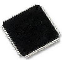
LH75411N0Q100C0 NXP Semiconductors, LH75411N0Q100C0 Datasheet - Page 29

LH75411N0Q100C0
Manufacturer Part Number
LH75411N0Q100C0
Description
MCU ARM7, LCD CTRL, SMD, LQFP144
Manufacturer
NXP Semiconductors
Datasheet
1.LH75411N0Q100C0.pdf
(63 pages)
Specifications of LH75411N0Q100C0
Core Size
32bit
No. Of I/o's
76
Ram Memory Size
32KB
Cpu Speed
84MHz
Oscillator Type
External Only
No. Of Timers
3
Digital Ic Case Style
LQFP
Supply Voltage Range
1.7V To 1.98V, 3V To 3.6V
Controller Family/series
LH75xxx
Peripherals
ADC, RTC, LVD
Rohs Compliant
Yes
Data Bus Width
32 bit
Program Memory Type
ROMLess
Data Ram Size
32 KB
Interface Type
JTAG, SCI, SPI, SSI, UART
Maximum Clock Frequency
84 MHz
Number Of Programmable I/os
76
Number Of Timers
3
Maximum Operating Temperature
+ 85 C
Mounting Style
SMD/SMT
Package / Case
LQFP
Minimum Operating Temperature
- 40 C
On-chip Adc
10 bit, 8 Channel
Lead Free Status / RoHS Status
Lead free / RoHS Compliant
Available stocks
Company
Part Number
Manufacturer
Quantity
Price
Company:
Part Number:
LH75411N0Q100C0
Manufacturer:
Sharp Microelectronics
Quantity:
10 000
Company:
Part Number:
LH75411N0Q100C0,55
Manufacturer:
NXP Semiconductors
Quantity:
10 000
System-on-Chip
CAN 2.0B FEATURES
• Full compliance with 2.0A and 2.0B Bosch
• Supports 11-bit and 29-bit identifiers
• Supports bit rates up to 1Mbit/s
• 64-byte receive FIFO
• Software-driven bit-rate detection for hot plug-in
• Single-shot transmission option
• Acceptance filtering
• Listen Only Mode
• Reception of ‘own’ messages
• Error interrupt generated for each CAN bus error
• Arbitration-lost interrupt with record of bit position
• Read/write error counters
• Last error register
• Programmable error-limit warning.
Analog-to-Digital Converter (ADC)/
Brownout Detector
nects as a slave to the APB. The ADC block consists of
an 8-channel, 10-bit Analog-to-Digital Converter with
integrated Touch Screen Controller. The complete
Touch Screen interface is achieved by combining the
front-end biasing, control circuitry with analog-to-digital
conversion, reference generation, and digital control.
clock derived from the system clock. The clock drives
the measurement sequencer and the successive-
approximation circuitry.
out Detector is an asynchronous comparator that com-
pares a divided version of the 3.3 V supply and a
bandgap-derived reference voltage. If the supply dips
below a Trip point, the Brownout Detector sets a status
register bit. The status bit is wired to the VIC and can
interrupt the processor core. This allows the Host Con-
troller to warn users of an impending shutdown and may
provide the ADC with sufficient time to save its state.
ADC/BROWNOUT DETECTOR FEATURES
• 10-bit fully differential Successive Approximation
• 8-channel multiplexer for routing user-selected inputs
• 16-entry × 16-bit-wide FIFO that holds the 10-bit
• Front bias-and-control network for Touch Screen
Preliminary data sheet
specifications
support
Register (SAR) with integrated sample/hold
to the ADC in Single Ended and Differential Modes
ADC output and a 4-bit tag number
interface and support functions compatible with indus-
try-standard 4- and 5-wire touch-sensitive panels
The ADC is an AMBA-compliant peripheral that con-
The ADC also has a programmable measurement
The ADC includes a Brownout Detector. The Brown-
NXP Semiconductors
Rev. 01 — 16 July 2007
• Touch-pressure sensing circuits
• Pen-down sensing circuit and interrupt generator
• Voltage-reference generator that is independently
• Conversion automation function to minimize control-
• Brownout Detector.
Synchronous Serial Port (SSP)
serial communication with slave peripheral devices that
have a Motorola SPI, National Semiconductor
Microwire, or Texas Instruments DSP-compatible
Synchronous Serial Interface (SSI).
data received from a peripheral device. The transmit and
receive paths are buffered with internal FIFO memories.
These memories store eight 16-bit values independently
in both transmit and receive modes. During transmission:
• Data writes to the transmit FIFO via the APB
• The transmit data is queued for parallel-to-serial
• The transmit logic formats the data into the appropri-
SSP FEATURES
• SSI in Master Only Mode. The SSP performs serial
• Two 16-bit-wide, 8-entry-deep FIFOs, one for data
• Supports interrupt-driven data transfers that are
• Programmable clock bit rate.
• Programmable data frame size, from 4 to 16 bits long,
• Four interrupts, each of which can be individually
• Loopback Test Mode.
controlled
ler interrupt overhead
interface.
conversion onto the transmit interface.
ate frame type:
communications as a master device in one of three
modes:
transmission and one for data reception.
greater than the FIFO watermark.
depending on the size of data programmed. Each
frame transmits starting with the most-significant bit.
enabled or disabled using the SSP Control Register
bits. A combined interrupt is also generated as an
OR function of the individual interrupt requests.
The SSP is a master-only interface for synchronous
The SSP performs serial-to-parallel conversion on
– Motorola SPI
– National Semiconductor Microwire
– Texas Instruments DSP-compatible SSI.
– Motorola SPI
– Texas Instruments DSP-compatible synchronous
– National Semiconductor Microwire.
serial interface
LH75401/LH75411
29


