GT15Q102 Toshiba, GT15Q102 Datasheet
GT15Q102
Specifications of GT15Q102
Available stocks


Related parts for GT15Q102

GT15Q102 Summary of contents
Page 1
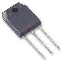
... Collector current 1 ms Collector power dissipation (Tc 25°C) Junction temperature Storage temperature range Silicon N Channel IGBT GT15Q102 = 2.7 V (max) Symbol Rating Unit V 1200 V CES GES 170 150 ° 55~150 °C stg 1 GT15Q102 Unit: mm JEDEC ― JEITA ― TOSHIBA 2-16C1C Weight: 4.6 g 2002-01-18 ...
Page 2
... V, V CES 1.5 mA (OFF (sat ies Inductive Load 600 off R th ( (off) 10% 10 GT15Q102 Min Typ 4.0 2.1 1 MHz 850 0.05 0.12 0.16 (Note1) 0.56 10% 90% 90% 10% 10 (on off on 2002-01-18 Max Unit 500 nA 1.0 mA 7 0.32 0.74 °C/W 10% ...
Page 3
... GE 20 Common emitter Tc 25° Gate-emitter voltage V ( – Common emitter 125° Gate-emitter voltage V ( Common emitter Tc 40° Gate-emitter voltage V 20 Common emitter Tc 125° Gate-emitter voltage V 4 Common emitter Case temperature Tc (°C) 3 GT15Q102 V – ( – ( – (sat 100 140 2002-01-18 ...
Page 4
... Tc 0.5 0 0.1 0.05 0 300 Switching loss Common emitter V CC 600 Note2 E off 1 0.5 0.3 0.1 300 500 0 4 GT15Q102 Switching time – 25°C 125° Collector current I (A) C Switching time – I off f C 25°C 125°C t off Collector current I ...
Page 5
... Common emitter 800 C ies Tc 25°C 600 600 400 oes 200 C res 0 300 1000 125°C 0 0.1 1000 3000 1 3 (V) Collector-emitter voltage GT15Q102 – 400 8 200 120 160 200 Gate charge Q (nC) G Reverse bias SOA 100 300 1000 3000 (V) CE 2002-01-18 ...
Page 6
... TOSHIBA CORPORATION for any infringements of intellectual property or other rights of the third parties which may result from its use. No license is granted by implication or otherwise under any intellectual property or other rights of TOSHIBA CORPORATION or others. The information contained herein is subject to change without notice. 6 GT15Q102 000707EAA 2002-01-18 ...