ETRX2HR-PA Telegesis Ltd, ETRX2HR-PA Datasheet - Page 25
ETRX2HR-PA
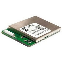
Manufacturer Part Number
ETRX2HR-PA
Description
MODULE
Manufacturer
Telegesis Ltd
Datasheet
1.ETRX2-PA.pdf
(33 pages)
Specifications of ETRX2HR-PA
Module Applications
AMR, Building Automation, Wireless Sensor Network, M2M Industrial Controls
Mcu Supported Families
EM250
Processor Type
EM250
Wireless Protocol
IEEE 802.15.4
Data Rate
250Kbps
Module Interface
I2C, SPI, UART
Rohs Compliant
Yes
Lead Free Status / RoHS Status
Lead free / RoHS Compliant


ETRX2PA
15 Recommended Footprint
In order to surface mount the module, we recommend that you use pads which are 1.5mm wide
and 1.7mm high, the extra height extending the pads shown in Figure 9 towards the outside of
your layout. You must retain the “keep-out” zone shown in Figure 5 (page 21), and ensure that this
area is free of copper tracks and/or copper planes/layers.
You must also ensure that there are no exposed pads or vias on your layout which may contact
with the pads (for the optional connector), or vias on the bottom surface of the ETRX2-PA module.
If the module is to be soldered by hand for prototyping we recommend that you increase the height
of the pads to allow easier access.
Figure 9: Recommended Footprint
The land pattern dimensions above serve as a guideline.
We recommend that you use the same pad dimensions for the solder paste screen as you have for
the copper pads. However these sizes and shapes may need to be varied depending on your
soldering processes and your individual production standards. We recommend a paste screen
thickness of 120µm to 150µm, although it may be necessary to go up to 200µm to ensure reliable
joints.
Although the under side of ETRX2-PA is fully coated (except for the footprint of the additional
Harwin SMT connector), no exposed copper, such as through-hole vias, planes or tracks on your
board component layer, should be located below the ETRX2-PA in order to avoid ‘shorts’. In
cases where a exposed track or through hole via has to be located under the module it must be
kept away from ETRX2-PA via holes. The ETRX2-PA multilayer PCB contains an inner RF
shielding ground plane, therefore there is no need to have an additional copper plane directly
under the ETRX2-PA.
©2009 Telegesis (UK) Ltd
- 25 -
ETRX2PA Product Manual (Rev 1.07)
Related parts for ETRX2HR-PA
Image
Part Number
Description
Manufacturer
Datasheet
Request
R

Part Number:
Description:
KIT DEVELOPMENT FOR ETRX357
Manufacturer:
Telegesis Ltd
Datasheet:

Part Number:
Description:
MODULE ZIGBEE USB STICK
Manufacturer:
Telegesis Ltd
Datasheet:

Part Number:
Description:
MODULE ZIGBEE PWR AMP USB STICK
Manufacturer:
Telegesis Ltd
Datasheet:

Part Number:
Description:
ZIGBEE ETHERNET ACCESS POINT
Manufacturer:
Telegesis Ltd
Datasheet:

Part Number:
Description:
ZIGBEE ETHERNET ACCESS POINT
Manufacturer:
Telegesis Ltd
Datasheet:

Part Number:
Description:
MODULE ZIGBEE EM357 W/CHIP ANT
Manufacturer:
Telegesis Ltd
Datasheet:

Part Number:
Description:
MODULE ZIGBEE EM250 CHIP ANT
Manufacturer:
Telegesis Ltd
Datasheet:

Part Number:
Description:
MODULE ZIGBEE W/PWR AMP
Manufacturer:
Telegesis Ltd
Datasheet:
Part Number:
Description:
MODULE ZIGBEE W/PA LNA CHIP ANT
Manufacturer:
Telegesis Ltd
Datasheet:
Part Number:
Description:
MODULE ZIGBEE W/PA LNA U.FL
Manufacturer:
Telegesis Ltd
Datasheet:
Part Number:
Description:
MODULE, ZIGBEE, ETRX351, CHIP ANT
Manufacturer:
Telegesis Ltd
Datasheet:
Part Number:
Description:
MODULE, ZIGBEE, ETRX3, HIROSE
Manufacturer:
Telegesis Ltd
Datasheet:
Part Number:
Description:
MODULE, ZIGBEE, ETRX3, PA+LNA, CHIP
Manufacturer:
Telegesis Ltd
Datasheet:
Part Number:
Description:
MODULE, ZIGBEE, ETRX3, PA+LNA, HIROS
Manufacturer:
Telegesis Ltd
Datasheet: