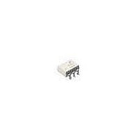
H11L1SVM Fairchild Semiconductor, H11L1SVM Datasheet - Page 3

H11L1SVM
Manufacturer Part Number
H11L1SVM
Description
High Speed Optocouplers Optocoupler Schmitt Trigger
Manufacturer
Fairchild Semiconductor
Datasheet
1.H11L1SR2VM.pdf
(10 pages)
Specifications of H11L1SVM
Isolation Voltage
5300 Vrms
Maximum Fall Time
0.1 us
Maximum Rise Time
0.1 us
Output Device
Logic Gate Photo IC
Configuration
1 Channel
Maximum Baud Rate
1 MBps
Maximum Forward Diode Voltage
1.5 V
Maximum Reverse Diode Voltage
6 V
Maximum Power Dissipation
250 mW
Maximum Operating Temperature
+ 85 C
Minimum Operating Temperature
- 40 C
Package / Case
PDIP W SMD
Lead Free Status / RoHS Status
Lead free / RoHS Compliant
Other names
H11L1SVM_NL
Available stocks
Company
Part Number
Manufacturer
Quantity
Price
©2005 Fairchild Semiconductor Corporation
H11L1M, H11L2M, H11L3M Rev. 1.0.3
Electrical Characteristics
Individual Component Characteristics
Transfer Characteristics
Isolation Characteristics
Note:
1. Maximum I
EMITTER
DETECTOR
DC CHARACTERISTICS
AC CHARACTERISTICS, Switching Speed
I
Symbol
Symbol
F(off)
Symbol
require the LED to be driven at a current greater than 1.6mA to guarantee the device will turn on. A 10% guard band is
recommended to account for degradation of the LED over its lifetime. The maximum allowable LED drive current is 60mA.
I
I
CC(off)
CC(on)
I
I
V
C
R
V
V
F(on)
F(off)
I
V
C
t
t
OH
I
ISO
on
off
t
ISO
ISO
CC
OL
t
R
/I
f
r
F
J
F(on)
F(ON)
Parameters
Input Forward Voltage
Reverse Current
Capacitance
Operating Voltage Range
Supply Current
Output Current, High
Parameter
Supply Current
Output Voltage, low
Turn-On Threshold Current
Turn-Off Threshold Current
Hysteresis Ratio
Turn-On time
Fall Time
Turn-Off Time
Rise time
Data Rate
Parameter
Input-Output Isolation Voltage
Isolation Capacitance
Isolation Resistance
is the maximum current required to trigger the output. For example, a 1.6mA maximum trigger current would
(T
A
(1)
= 25°C Unless otherwise specified.)
I
I
V
V = 0, f = 1.0MHz
I
I
I
R
I
R
R
R
R
I
R
I
R
I
R
I
F
F
F
F
F
F
F
F
F
F
R
L
L
L
L
L
L
L
L
Test Conditions
= 10mA
= 0.3mA
= 0, V
= 0, V
Test Conditions
= 10mA, V
= I
= I
= I
= I
= I
= 270 ,V
= 270 , V
= 270 , V
= 270 , V
= 270 , V
= 270 , V
= 270 , V
= 270 , V
= 3V
t =1 sec.
V
V
F(on)
F(on)
F(on)
F(on)
F(on)
I-O
I-O
Test Conditions
= 0V, f = 1MHz
= ±500 VDC
CC
CC
, T
, T
, T
, T
max.
= 5V
= V
A
A
A
A
= 25°C
= 25°C
3
CC
CC
CC
= 25°C
= 25°C
CC
CC
CC
CC
CC
CC
O
= 5V,
= 5V,
= 5V
= 5V
= 5V
= 5V
= 5V,
= 5V,
= 5V,
= 15V
H11L1M
H11L2M
H11L3M
Device
Device
All
All
All
All
All
All
All
All
All
All
All
All
All
All
All
Min.
7500
10
11
Min.
0.75
Min.
0.50
0.3
3
Typ.
0.4
Typ.
Typ.
1.2
1.0
1.6
0.75
1.6
0.2
1.0
1.0
0.1
1.2
0.1
1.0
Max.
0.6
Max.
100
100
Max.
1.5
5.0
10
15
10.0
0.90
5.0
0.4
1.6
5.0
www.fairchildsemi.com
4
4
Units
V
Units
PEAK
Units
pF
mA
MHz
µA
pF
µA
mA
mA
mA
V
V
µs
µs
µs
µs
V


