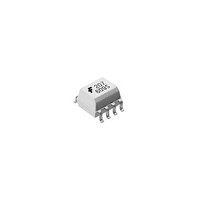
MOC213R1VM Fairchild Semiconductor, MOC213R1VM Datasheet - Page 5

MOC213R1VM
Manufacturer Part Number
MOC213R1VM
Description
Transistor Output Optocouplers Optocoupler Phototransistor
Manufacturer
Fairchild Semiconductor
Datasheet
1.MOC213M.pdf
(10 pages)
Specifications of MOC213R1VM
Maximum Input Diode Current
60 mA
Maximum Reverse Diode Voltage
6 V
Output Device
Phototransistor
Output Type
DC
Configuration
1 Channel
Input Type
DC
Maximum Collector Emitter Voltage
30 V
Maximum Collector Emitter Saturation Voltage
0.4 V
Isolation Voltage
2500 Vrms
Maximum Forward Diode Voltage
1.5 V
Maximum Collector Current
150 mA
Maximum Power Dissipation
250 mW
Maximum Operating Temperature
+ 100 C
Minimum Operating Temperature
- 40 C
Package / Case
SOIC-8 Narrow
Lead Free Status / RoHS Status
Lead free / RoHS Compliant
Available stocks
Company
Part Number
Manufacturer
Quantity
Price
Part Number:
MOC213R1VM
Manufacturer:
FAIRCHILD/仙童
Quantity:
20 000
©2005 Fairchild Semiconductor Corporation
MOC211M, MOC212M, MOC213M Rev. 1.0.1
Typical Performance Curves
INPUT
1.0
0.9
0.8
0.7
0.6
0.5
0.4
0.3
0.2
0.1
0.0
10
I
F
I
F
= 20mA
TEST CIRCUIT
Fig. 7 CTR vs. R BE (Saturated)
R
R
BE
BE
–
BASE RESISTANCE (k )
100
I
V
C
Figure 10. Switching Time Test Circuit and Waveforms
V
Normalized to:
CTR at R
CC
CE
= 0.3V, T
= 10V
1.6
1.4
1.2
1.0
0.8
0.6
0.4
0.2
0.0
I
OUTPUT
I
F
R
F
0.01
BE
= 10mA
= 5mA
L
Adjust I
= Open
V
I
R
NORMALIZED TO :
t
C
of f f
A
CC
L
= 2mA
= 25 C
(Continued)
= 100
AT R
= 10V
BE
F
to produce I
= OPEN
R
Fig. 9 Normalized t off vs. R BE
0.1
BE
1000
– BASE RESISTANCE
C
= 2mA
5
1
4.0
3.5
3.0
2.5
2.0
1.5
1.0
0.5
0.0
0.01
(M )
10%
90%
10
V
I
R
NORMALIZED TO :
t
C
on
CC
L
= 2mA
= 100
AT R
t
on
= 10V
BE
WAVEFORMS
= OPEN
R
Fig. 8 Normalized t on vs. R BE
0.1
BE
100
–
BASE RESISTANCE (M )
t
r
1
t
t
f
off
INPUT PULSE
OUTPUT PULSE
10
www.fairchildsemi.com
100


