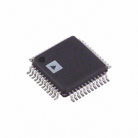
AD9753ASTZRL Analog Devices Inc, AD9753ASTZRL Datasheet - Page 11

AD9753ASTZRL
Manufacturer Part Number
AD9753ASTZRL
Description
12-Bit, 300 MSPS TxDAC+ DAC
Manufacturer
Analog Devices Inc
Series
TxDAC+®r
Datasheet
1.AD9753ASTZ.pdf
(28 pages)
Specifications of AD9753ASTZRL
Settling Time
11ns
Number Of Bits
12
Data Interface
Parallel
Number Of Converters
1
Voltage Supply Source
Analog and Digital
Power Dissipation (max)
165mW
Operating Temperature
-40°C ~ 85°C
Mounting Type
Surface Mount
Package / Case
48-LQFP
Lead Free Status / RoHS Status
Lead free / RoHS Compliant
For Use With
AD9753-EB - BOARD EVAL FOR AD9753
Lead Free Status / RoHS Status
Lead free / RoHS Compliant
Available stocks
Company
Part Number
Manufacturer
Quantity
Price
Company:
Part Number:
AD9753ASTZRL
Manufacturer:
Analog Devices Inc
Quantity:
10 000
REFERENCE CONTROL AMPLIFIER
The AD9753 also contains an internal control amplifier that is
used to regulate the DAC’s full-scale output current, I
The control amplifier is configured as a voltage-to-current
converter as shown in Figure 4, so that its current output, I
determined by the ratio of V
as stated in Equation 4. I
sources with the proper scaling factor to set I
Equation 3.
The control amplifier allows a wide (10:1) adjustment span of
I
62.5 µA and 625 µA. The wide adjustment span of I
provides several application benefits. The first benefit relates
directly to the power dissipation of the AD9753, which is
proportional to I
The second benefit relates to the 20 dB adjustment, which is
useful for system gain control purposes.
The small signal bandwidth of the reference control amplifier is
approximately 500 kHz and can be used for low frequency,
small signal multiplying applications.
PLL CLOCK MULTIPLIER OPERATION
The Phase-Locked Loop (PLL) is intrinsic to the operation of
the AD9753 in that it produces the necessary internally syn-
chronized 2× clock for the edge-triggered latches, multiplexer,
and DAC.
With PLLVDD connected to its supply voltage, the AD9753 is
in PLL mode. Figure 6 shows a functional block diagram of the
AD9753 clock control circuitry with PLL active. The circuitry
consists of a phase detector, charge pump, voltage controlled
oscillator (VCO), input data rate range control, clock logic
circuitry, and control input/outputs. The ÷ 2 logic in the feed-
back loop allows the PLL to generate the 2× clock needed for
the DAC output latch.
Figure 7 defines the input and output timing for the AD9753
with the PLL active. CLK in Figure 7 represents the clock
that is generated external to the AD9753. The input data at
both Ports 1 and 2 is latched on the same CLK rising edge.
CLK may be applied as a single-ended signal by tying CLK– to
midsupply and applying CLK to CLK+, or as a differential
signal applied to CLK+ and CLK–.
RESET has no purpose when using the internal PLL and should
be grounded. When the AD9753 is in PLL mode, PLLLOCK
is the output of the internal phase detector. When locked, the
lock output in this mode will be a Logic 1.
REV. B
OUTFS
CLK+
CLK–
over a 2 mA to 20 mA range by setting I
DIFFERENTIAL-
SINGLE-ENDED
Figure 6. Clock Circuitry with PLL Active
AMP
TO-
(3.0V TO 3.6V)
OUTFS
AD9753
CLKVDD
TO INPUT
LATCHES
DETECTOR
(refer to the Power Dissipation section).
PHASE
REF
PLLLOCK
REFIO
is applied to the segmented current
and an external resistor, R
CHARGE
PUMP
TO DAC
LATCH
2
LPF
( 1, 2, 4, 8)
CONTROL
392
OUTFS
CLKCOM
RANGE
VCO
PLLVDD
REF
1.0
, as stated in
between
F
OUTFS
REF
OUTFS
DIV0
DIV1
3.0V TO
3.6V
, is
SET
.
,
–11–
Typically, the VCO can generate outputs of 100 MHz to
400 MHz. The range control is used to keep the VCO operating
within its designed range, while allowing input clocks as low as
6.25 MHz. With the PLL active, logic levels at DIV0 and DIV1
determine the divide (prescaler) ratio of the range controller.
Table I gives the frequency range of the input clock for the
different states of DIV0 and DIV1.
CLK Frequency
50 MHz–150 MHz
25 MHz–100 MHz
12.5 MHz–50 MHz
6.25 MHz–25 MHz
A 392 Ω resistor and 1.0 µF capacitor connected in series from
LPF to PLLVDD are required to optimize the phase noise versus
the settling/acquisition time characteristics of the PLL. To
obtain optimum noise and distortion performance, PLLVDD
should be set to a voltage level similar to DVDD and
CLKVDD.
In general, the best phase noise performance for any PLL range
control setting is achieved with the VCO operating near its maxi-
mum output frequency of 400 MHz.
As stated earlier, applications requiring input data rates below
6.25 MSPS must disable the PLL clock multiplier and provide
an external 2× reference clock. At higher data rates however,
applications already containing a low phase noise (i.e., jitter)
Table I. CLK Rates for DIV0, DIV1 Levels with PLL Active
I
OUTA
I
OUTA
Figure 7a. DAC Input Timing Requirements with
PLL Active, Single Clock Cycle
Figure 7b. DAC Input Timing Requirements with
PLL Active, Multiple Clock Cycles
OR I
DATA IN
PORT 1
PORT 2
DATA IN
OR I
PORT 1
PORT 2
OUTB
CLK
OUTB
CLK
t
DATA X
DATA Y
S
DATA X
DATA W
t
DIV1
0
0
1
1
t
H
1/2 CYCLE +
LPW
XXX
DATA W
DIV0
0
1
0
1
t
PD
DATA Y
DATA Z
DATA X
DATA X
Range Controller
÷ 1
÷ 2
÷ 4
÷ 8
DATA Y
AD9753
t
PD
DATA Z
DATA Y


