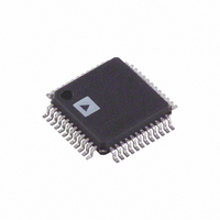
AD9753ASTZRL Analog Devices Inc, AD9753ASTZRL Datasheet - Page 17

AD9753ASTZRL
Manufacturer Part Number
AD9753ASTZRL
Description
12-Bit, 300 MSPS TxDAC+ DAC
Manufacturer
Analog Devices Inc
Series
TxDAC+®r
Datasheet
1.AD9753ASTZ.pdf
(28 pages)
Specifications of AD9753ASTZRL
Settling Time
11ns
Number Of Bits
12
Data Interface
Parallel
Number Of Converters
1
Voltage Supply Source
Analog and Digital
Power Dissipation (max)
165mW
Operating Temperature
-40°C ~ 85°C
Mounting Type
Surface Mount
Package / Case
48-LQFP
Lead Free Status / RoHS Status
Lead free / RoHS Compliant
For Use With
AD9753-EB - BOARD EVAL FOR AD9753
Lead Free Status / RoHS Status
Lead free / RoHS Compliant
Available stocks
Company
Part Number
Manufacturer
Quantity
Price
Company:
Part Number:
AD9753ASTZRL
Manufacturer:
Analog Devices Inc
Quantity:
10 000
passive reconstruction filter or cable. R
transformer’s impedance ratio and provides the proper source
termination that results in a low VSWR.
DIFFERENTIAL COUPLING USING AN OP AMP
An op amp can also be used to perform a differential-to-
single-ended conversion, as shown in Figure 21. The AD9753 is
configured with two equal load resistors, R
differential voltage developed across I
verted to a single-ended signal via the differential op amp
configuration. An optional capacitor can be installed across
I
addition of this capacitor also enhances the op amp’s distor-
tion performance by preventing the DAC’s high slewing output
from overloading the op amp’s input.
The common-mode rejection of this configuration is typically
determined by the resistor matching. In this circuit, the dif-
ferential op amp circuit using the AD8047 is configured to
provide some additional signal gain. The op amp must operate
from a dual supply since its output is approximately ± 1.0 V.
A high speed amplifier capable of preserving the differential
performance of the AD9753, while meeting other system level
objectives (i.e., cost, power), should be selected. The op amp’s
differential gain, its gain setting resistor values, and full-scale
output swing capabilities should all be considered when opti-
mizing this circuit.
The differential circuit shown in Figure 22 provides the neces-
sary level-shifting required in a single-supply system. In this
case, AVDD, which is the positive analog supply for both the
AD9753 and the op amp, is also used to level-shift the differen-
tial output of the AD9753 to midsupply (i.e., AVDD/2). The
AD8041 is a suitable op amp for this application.
SINGLE-ENDED UNBUFFERED VOLTAGE OUTPUT
Figure 23 shows the AD9753 configured to provide a unipolar
output range of approximately 0 V to 0.5 V for a doubly termi-
nated 50 Ω cable since the nominal full-scale current, I
20 mA flows through the equivalent R
REV. B
OUTA
Figure 22. Single-Supply DC Differential Coupled Circuit
Figure 21. DC Differential Coupling Using an Op Amp
and I
AD9753
AD9753
OUTB
I
I
OUTA
OUTB
I
I
OUTB
OUTA
, forming a real pole in a low-pass filter. The
25
25
C
OPT
C
OPT
25
225
225
25
225
225
500
500
LOAD
DIFF
OUTA
AD8041
500
is determined by the
of 25 Ω. In this case,
LOAD
and I
1k
AD8047
500
, of 25 Ω. The
OUTB
AVDD
OUTFS
is con-
, of
–17–
R
I
ACOM directly or via a matching R
I
ance range is adhered to. One additional consideration in this
mode is the integral nonlinearity (INL), as discussed in the Analog
Outputs section. For optimum INL performance, the single-
ended, buffered voltage output configuration is suggested.
SINGLE-ENDED BUFFERED VOLTAGE OUTPUT
Figure 24 shows a buffered single-ended output configuration in
which the op amp performs an I–V conversion on the AD9753
output current. The op amp maintains I
virtual ground, thus minimizing the nonlinear output imped-
ance effect on the DAC’s INL performance as discussed in the
Analog Outputs section. Although this single-ended configura-
tion typically provides the best dc linearity performance, its ac
distortion performance at higher DAC update rates may be
limited by the op amp’s slewing capabilities. The op amp pro-
vides a negative unipolar output voltage and its full-scale output
voltage is simply the product of R
output should be set within the op amp’s voltage output swing
capabilities by scaling I
distortion performance may result with a reduced I
the signal current the op amp will be required to sink will
subsequently be reduced.
POWER AND GROUNDING CONSIDERATIONS, POWER
SUPPLY REJECTION
Many applications seek high speed and high performance under
less than ideal operating conditions. In these applications, the
implementation and construction of the printed circuit board is
as important as the circuit design. Proper RF techniques must
be used for device selection, placement, and routing, as well as
power supply bypassing and grounding, to ensure optimum
performance. Figures 34 to 41 illustrate the recommended
printed circuit board ground, power, and signal plane layouts
that are implemented on the AD9753 evaluation board.
One factor that can measurably affect system performance is the
ability of the DAC output to reject dc variations or ac noise
superimposed on the analog or digital dc power distribution.
OUTB
OUTFS
LOAD
Figure 23. 0 V to 0.5 V Unbuffered Voltage Output
AD9753
. The unused output (I
represents the equivalent load resistance seen by I
and R
Figure 24. Unipolar Buffered Voltage Output
AD9753
I
I
OUTB
OUTA
LOAD
I
I
OUTA
OUTB
can be selected as long as the positive compli-
I
OUTFS
OUTFS
200
25
= 20mA
OUTA
and/or R
50
FB
or I
200
C
R
OPT
and I
FB
LOAD
OUTB
FB
. An improvement in ac
OUTFS
OUTA
. Different values of
) can be connected to
V
OUTA
V
OUT
. The full-scale
(or I
AD9753
50
= 0V TO 0.5V
= I
OUTFS
OUTB
OUTFS
, since
OUTA
) at a
R
FB
or


