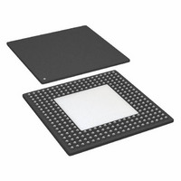
ADSP-21368BBPZ-2A Analog Devices Inc, ADSP-21368BBPZ-2A Datasheet - Page 14

ADSP-21368BBPZ-2A
Manufacturer Part Number
ADSP-21368BBPZ-2A
Description
IC,DSP,32-BIT,CMOS,BGA,256PIN,PLASTIC
Manufacturer
Analog Devices Inc
Series
SHARC®r
Type
Floating Pointr
Datasheet
1.ADSP-21369KBPZ-2A.pdf
(60 pages)
Specifications of ADSP-21368BBPZ-2A
Interface
DAI, DPI
Clock Rate
333MHz
Non-volatile Memory
ROM (768 kB)
On-chip Ram
256kB
Voltage - I/o
3.30V
Voltage - Core
1.20V
Operating Temperature
-40°C ~ 85°C
Mounting Type
Surface Mount
Package / Case
256-BGA Exposed Pad, 256-eBGA, 256-HBGA
Device Core Size
32/40Bit
Architecture
Super Harvard
Format
Floating Point
Clock Freq (max)
333MHz
Mips
333
Device Input Clock Speed
333MHz
Ram Size
256KB
Program Memory Size
768KB
Operating Supply Voltage (typ)
1.2/3.3V
Operating Supply Voltage (min)
1.14/3.13V
Operating Supply Voltage (max)
1.26/3.47V
Operating Temp Range
-40C to 85C
Operating Temperature Classification
Industrial
Mounting
Surface Mount
Pin Count
256
Package Type
SBGA
Lead Free Status / RoHS Status
Lead free / RoHS Compliant
Lead Free Status / RoHS Status
Lead free / RoHS Compliant
Available stocks
Company
Part Number
Manufacturer
Quantity
Price
Company:
Part Number:
ADSP-21368BBPZ-2A
Manufacturer:
Analog Devices Inc
Quantity:
10 000
ADSP-21367/ADSP-21368/ADSP-21369
Table 8. Pin Descriptions (Continued)
Name
SDRAS
SDCAS
SDWE
SDCKE
SDA10
SDCLK0
SDCLK1
DAI _P
DPI _P
TDI
TDO
TMS
TCK
TRST
14–1
20–1
Type
O/T (pu)
O/T (pu)
O/T (pu)
O/T (pu)
O/T (pu)
O/T
O/T
I/O with pro-
grammable
pu
I/O with pro-
grammable
pu
I (pu)
O/T
I (pu)
I
I (pu)
2
2
1
1
1
1
1
State During/
After Reset
(ID = 00x)
Pulled high/
driven high
Pulled high/
driven high
Pulled high/
driven high
Pulled high/
driven high
Pulled high/
driven low
High-Z/driving
Pulled high/
pulled high
Pulled high/
pulled high
Rev. E | Page 14 of 60 | July 2009
Description
SDRAM Row Address Strobe. Connect to SDRAM’s RAS pin. In conjunction with other
SDRAM command pins, defines the operation for the SDRAM to perform.
SDRAM Column Address Select. Connect to SDRAM’s CAS pin. In conjunction with other
SDRAM command pins, defines the operation for the SDRAM to perform.
SDRAM Write Enable. Connect to SDRAM’s WE or W buffer pin.
SDRAM Clock Enable. Connect to SDRAM’s CKE pin. Enables and disables the CLK signal.
For details, see the data sheet supplied with the SDRAM device.
SDRAM A10 Pin. Enables applications to refresh an SDRAM in parallel with non-
SDRAM accesses. This pin replaces the DSP’s A10 pin only during SDRAM accesses.
SDRAM Clock Output 0. Clock driver for this pin differs from all other clock drivers. See
Figure 39 on Page
SDRAM Clock Output 1. Additional clock for SDRAM devices. For systems with multiple
SDRAM devices, handles the increased clock load requirements, eliminating need of off-
chip clock buffers. Either SDCLK1 or both SDCLKx pins can be three-stated. Clock driver
for this pin differs from all other clock drivers. See
The SDCLK1 signal is only available on the SBGA package. SDCLK1 is not available on the
LQFP_EP package.
Digital Applications Interface. These pins provide the physical interface to the DAI SRU.
The DAI SRU configuration registers define the combination of on-chip audiocentric
peripheral inputs or outputs connected to the pin, and to the pin’s output enable. The
configuration registers then determines the exact behavior of the pin. Any input or
output signal present in the DAI SRU may be routed to any of these pins. The DAI SRU
provides the connection from the serial ports (8), the SRC module, the S/PDIF module,
input data ports (2), and the precision clock generators (4), to the DAI_P20–1 pins. Pull-
ups can be disabled via the DAI_PIN_PULLUP register.
Digital Peripheral Interface. These pins provide the physical interface to the DPI SRU.
The DPI SRU configuration registers define the combination of on-chip peripheral inputs
or outputs connected to the pin and to the pin’s output enable. The configuration
registers of these peripherals then determines the exact behavior of the pin. Any input
or output signal present in the DPI SRU may be routed to any of these pins. The DPI SRU
provides the connection from the timers (3), SPIs (2), UARTs (2), flags (12) TWI (1), and
general-purpose I/O (9) to the DPI_P14–1 pins. The TWI output is an open-drain output—
so the pins used for I
be disabled via the DPI_PIN_PULLUP register.
Test Data Input (JTAG). Provides serial data for the boundary scan logic.
Test Data Output (JTAG). Serial scan output of the boundary scan path.
Test Mode Select (JTAG). Used to control the test state machine.
Test Clock (JTAG). Provides a clock for JTAG boundary scan. TCK must be asserted (pulsed
low) after power-up, or held low for proper operation of the processor
Test Reset (JTAG). Resets the test state machine. TRST must be asserted (pulsed low) after
power-up or held low for proper operation of the processor.
48.
2
C data and clock should be connected to logic level 0. Pull-ups can
Figure 39 on Page
48.


