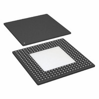
ADSP-21368BBPZ-2A Analog Devices Inc, ADSP-21368BBPZ-2A Datasheet - Page 3

ADSP-21368BBPZ-2A
Manufacturer Part Number
ADSP-21368BBPZ-2A
Description
IC,DSP,32-BIT,CMOS,BGA,256PIN,PLASTIC
Manufacturer
Analog Devices Inc
Series
SHARC®r
Type
Floating Pointr
Datasheet
1.ADSP-21369KBPZ-2A.pdf
(60 pages)
Specifications of ADSP-21368BBPZ-2A
Interface
DAI, DPI
Clock Rate
333MHz
Non-volatile Memory
ROM (768 kB)
On-chip Ram
256kB
Voltage - I/o
3.30V
Voltage - Core
1.20V
Operating Temperature
-40°C ~ 85°C
Mounting Type
Surface Mount
Package / Case
256-BGA Exposed Pad, 256-eBGA, 256-HBGA
Device Core Size
32/40Bit
Architecture
Super Harvard
Format
Floating Point
Clock Freq (max)
333MHz
Mips
333
Device Input Clock Speed
333MHz
Ram Size
256KB
Program Memory Size
768KB
Operating Supply Voltage (typ)
1.2/3.3V
Operating Supply Voltage (min)
1.14/3.13V
Operating Supply Voltage (max)
1.26/3.47V
Operating Temp Range
-40C to 85C
Operating Temperature Classification
Industrial
Mounting
Surface Mount
Pin Count
256
Package Type
SBGA
Lead Free Status / RoHS Status
Lead free / RoHS Compliant
Lead Free Status / RoHS Status
Lead free / RoHS Compliant
Available stocks
Company
Part Number
Manufacturer
Quantity
Price
Company:
Part Number:
ADSP-21368BBPZ-2A
Manufacturer:
Analog Devices Inc
Quantity:
10 000
GENERAL DESCRIPTION
The ADSP-21367/ADSP-21368/ADSP-21369 SHARC
sors are members of the SIMD SHARC family of DSPs that
feature Analog Devices’ Super Harvard Architecture. These pro-
cessors are source code-compatible with the ADSP-2126x and
ADSP-2116x DSPs as well as with first generation ADSP-2106x
SHARC processors in SISD (single-instruction, single-data)
mode. The processors are 32-bit/40-bit floating-point proces-
sors optimized for high performance automotive audio
applications with its large on-chip SRAM, mask programmable
ROM, multiple internal buses to eliminate I/O bottlenecks, and
an innovative digital applications interface (DAI).
As shown in the functional block diagram
processors use two computational units to deliver a significant
performance increase over the previous SHARC processors on a
range of DSP algorithms. Fabricated in a state-of-the-art, high
speed, CMOS process, the ADSP-21367/ADSP-21368/
ADSP-21369 processors achieve an instruction cycle time of up
to 2.5 ns at 400 MHz. With its SIMD computational hardware,
the processors can perform 2.4 GFLOPS running at 400 MHz.
Table 1
Table 1. Processor Benchmarks (at 400 MHz)
1
Table 2. ADSP-2136x Family Features
Benchmark Algorithm
1024 Point Complex FFT (Radix 4, with reversal) 23.2 s
FIR Filter (per tap)
IIR Filter (per biquad)
Matrix Multiply (pipelined)
Divide (y/x)
Inverse Square Root
Assumes two files in multichannel SIMD mode.
Feature
Frequency
RAM
ROM
Audio Decoders in ROM
Pulse-Width Modulation
S/PDIF
SDRAM Memory Bus Width
[3×3] × [3×1]
[4×4] × [4×1]
2
shows performance benchmarks for these devices.
1
1
1
32/16 bits
400 MHz
on Page
2M bits
6M bits
Yes
Yes
Yes
Speed
(at 400 MHz)
1.25 ns
5.0 ns
11.25 ns
20.0 ns
8.75 ns
13.5 ns
1, the
Rev. E | Page 3 of 60 | July 2009
®
proces-
ADSP-21367/ADSP-21368/ADSP-21369
Table 2. ADSP-2136x Family Features
1
2
The diagram
up the ADSP-21367/ADSP-21368/ADSP-21369 processors. The
core clock domain contains the following features.
W = Automotive grade product. See
Audio decoding algorithms include PCM, Dolby Digital EX, Dolby Prologic IIx,
Feature
Serial Ports
IDP
DAI
UART
DAI and DPI
S/PDIF Transceiver
AMI Interface Bus Width
SPI
TWI
SRC Performance
Package
information.
DTS 96/24, Neo:6, DTS ES, MPEG-2 AAC, MP3, and functions like bass
management, delay, speaker equalization, graphic equalization, and more.
Decoder/post-processor algorithm combination support varies depending upon
the chip version and the system configurations. Please visit www.analog.com for
complete information.
• Two processing elements (PEx, PEy), each of which com-
• Data address generators (DAG1, DAG2)
• Program sequencer with instruction cache
• PM and DM buses capable of supporting 2x64-bit data
• One periodic interval timer with pinout
• On-chip SRAM (2M bit)
• On-chip mask-programmable ROM (6M bit)
• JTAG test access port for emulation and boundary scan.
prises an ALU, multiplier, shifter, and data register file
transfers between memory and the core at every core pro-
cessor cycle
The JTAG provides software debug through user break-
points which allows flexible exception handling.
on Page 1
shows the two clock domains that make
256 Ball-
BGA,
208-Lead
LQFP_EP
Automotive Products on Page 58
1
32/16/8 bits
(Continued)
256 Ball-
BGA
128 dB
Yes
Yes
Yes
Yes
8
2
1
2
256 Ball-
BGA,
208-Lead
LQFP_EP
for more


