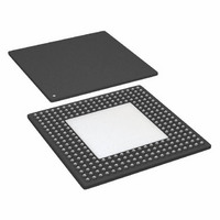
ADSP-21368BBPZ-2A Analog Devices Inc, ADSP-21368BBPZ-2A Datasheet - Page 39

ADSP-21368BBPZ-2A
Manufacturer Part Number
ADSP-21368BBPZ-2A
Description
IC,DSP,32-BIT,CMOS,BGA,256PIN,PLASTIC
Manufacturer
Analog Devices Inc
Series
SHARC®r
Type
Floating Pointr
Datasheet
1.ADSP-21369KBPZ-2A.pdf
(60 pages)
Specifications of ADSP-21368BBPZ-2A
Interface
DAI, DPI
Clock Rate
333MHz
Non-volatile Memory
ROM (768 kB)
On-chip Ram
256kB
Voltage - I/o
3.30V
Voltage - Core
1.20V
Operating Temperature
-40°C ~ 85°C
Mounting Type
Surface Mount
Package / Case
256-BGA Exposed Pad, 256-eBGA, 256-HBGA
Device Core Size
32/40Bit
Architecture
Super Harvard
Format
Floating Point
Clock Freq (max)
333MHz
Mips
333
Device Input Clock Speed
333MHz
Ram Size
256KB
Program Memory Size
768KB
Operating Supply Voltage (typ)
1.2/3.3V
Operating Supply Voltage (min)
1.14/3.13V
Operating Supply Voltage (max)
1.26/3.47V
Operating Temp Range
-40C to 85C
Operating Temperature Classification
Industrial
Mounting
Surface Mount
Pin Count
256
Package Type
SBGA
Lead Free Status / RoHS Status
Lead free / RoHS Compliant
Lead Free Status / RoHS Status
Lead free / RoHS Compliant
Available stocks
Company
Part Number
Manufacturer
Quantity
Price
Company:
Part Number:
ADSP-21368BBPZ-2A
Manufacturer:
Analog Devices Inc
Quantity:
10 000
Parallel Data Acquisition Port (PDAP)
The timing requirements for the PDAP are provided in
Table
the IDP. For details on the operation of the IDP, see the IDP
Table 33. Parallel Data Acquisition Port (PDAP)
1
Parameter
Timing Requirements
t
t
t
t
t
t
Switching Characteristics
t
t
Data Source pins are DATA31–12, or DAI pins. Source pins for SCLK and FS are: 1) DATA11–10 pins, 2) DAI pins.
SPCLKEN
HPCLKEN
PDSD
PDHD
PDCLKW
PDCLK
PDHLDD
PDSTRB
1
1
1
1
33. PDAP is the parallel mode operation of Channel 0 of
PDAP_CLKEN Setup Before PDAP_CLK Sample Edge
PDAP_CLKEN Hold After PDAP_CLK Sample Edge
PDAP_DAT Setup Before SCLK PDAP_CLK Sample Edge
PDAP_DAT Hold After SCLK PDAP_CLK Sample Edge
Clock Width
Clock Period
Delay of PDAP Strobe After Last PDAP_CLK Capture Edge for a Word
PDAP Strobe Pulse Width
(PDAP_STROBE)
(PDAP_CLKEN)
(PDAP_CLK)
DAI_P20–1
DAI_P20–1
DAI_P20–1
DATA
SAMPLE EDGE
Rev. E | Page 39 of 60 | July 2009
t
PDCLKW
Figure 26. PDAP Timing
t
SPCLKEN
t
PDSD
t
PDHLDD
ADSP-21367/ADSP-21368/ADSP-21369
chapter of the ADSP-21368 SHARC Processor Hardware
Reference. Note that the 20 bits of external PDAP data can be
provided through the external port DATA31–12 pins or the
DAI pins.
t
t
t
HPCLKEN
PDHD
PDCLK
t
PDSTRB
Min
2.5
2.5
3.85
2.5
(t
t
2 × t
2 × t
PCLK
PCLK
× 4
× 4) ÷ 2 – 3
PCLK
PCLK
+ 3
– 1
Max
Unit
ns
ns
ns
ns
ns
ns
ns
ns


