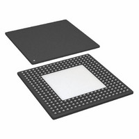
ADSP-21368BBPZ-2A Analog Devices Inc, ADSP-21368BBPZ-2A Datasheet - Page 19

ADSP-21368BBPZ-2A
Manufacturer Part Number
ADSP-21368BBPZ-2A
Description
IC,DSP,32-BIT,CMOS,BGA,256PIN,PLASTIC
Manufacturer
Analog Devices Inc
Series
SHARC®r
Type
Floating Pointr
Datasheet
1.ADSP-21369KBPZ-2A.pdf
(60 pages)
Specifications of ADSP-21368BBPZ-2A
Interface
DAI, DPI
Clock Rate
333MHz
Non-volatile Memory
ROM (768 kB)
On-chip Ram
256kB
Voltage - I/o
3.30V
Voltage - Core
1.20V
Operating Temperature
-40°C ~ 85°C
Mounting Type
Surface Mount
Package / Case
256-BGA Exposed Pad, 256-eBGA, 256-HBGA
Device Core Size
32/40Bit
Architecture
Super Harvard
Format
Floating Point
Clock Freq (max)
333MHz
Mips
333
Device Input Clock Speed
333MHz
Ram Size
256KB
Program Memory Size
768KB
Operating Supply Voltage (typ)
1.2/3.3V
Operating Supply Voltage (min)
1.14/3.13V
Operating Supply Voltage (max)
1.26/3.47V
Operating Temp Range
-40C to 85C
Operating Temperature Classification
Industrial
Mounting
Surface Mount
Pin Count
256
Package Type
SBGA
Lead Free Status / RoHS Status
Lead free / RoHS Compliant
Lead Free Status / RoHS Status
Lead free / RoHS Compliant
Available stocks
Company
Part Number
Manufacturer
Quantity
Price
Company:
Part Number:
ADSP-21368BBPZ-2A
Manufacturer:
Analog Devices Inc
Quantity:
10 000
The VCO frequency is calculated as follows:
f
f
where:
f
PLLM = Multiplier value programmed in the PMCTL register.
During reset, the PLLM value is derived from the ratio selected
using the CLK_CFG pins in hardware.
PLLD = Divider value 1, 2, 4, or 8 based on the PLLD value pro-
grammed on the PMCTL register. During reset this value is 1.
f
f
f
VCO
CCLK
VCO
INPUT
INPUT
INPUT
• The product of CLKIN and PLLM must never exceed f
= 2 PLLM f
= VCO output
(max) in
(INDIV = 1).
= (2 PLLM f
XTAL
= Input frequency to the PLL.
= CLKIN when the input divider is disabled or
= CLKIN 2 when the input divider is enabled
BUF
CLKIN
Table 13
4096 CLKIN
DELAY OF
CYCLES
INPUT
INPUT
if the input divider is enabled
DIVIDER
CLKIN
PMCTL
(INDIV)
) (2 PLLD)
f
INPUT
Figure 5. Core Clock and System Clock Relationship to CLKIN
CLK_CFGx/PMCTL (2xPLLM)
FILTER
LOOP
MULTIPLIER
CLKOUT (TEST ONLY)
PLL
Rev. E | Page 19 of 60 | July 2009
PLL
VCO
VCO
f
VCO
DIVIDER
(2xPLLD)
PMCTL
PLL
ADSP-21367/ADSP-21368/ADSP-21369
Note the definitions of the clock periods that are a function of
CLKIN and the appropriate ratio control shown in and
Table
peripherals are defined in relation to t
cific timing section for each peripheral’s timing information.
Table 11. Clock Periods
Figure 5
lator or crystal. The shaded divider/multiplier blocks denote
where clock ratios can be set through hardware or software
using the power management control register (PMCTL). For
more information, see the processor hardware reference.
Timing
Requirements
t
t
t
CK
CCLK
PCLK
f
CCLK
11. All of the timing specifications for the ADSP-2136x
(PLLBP)
PMCTL
shows core to CLKIN relationships with external oscil-
CCLK
(SDCKR)
DIVIDER
Description
CLKIN Clock Period
Processor Core Clock Period
Peripheral Clock Period = 2 × t
SDRAM
PMCTL
DIVIDE
BY 2
BUF
PCLK
PCLK
(PLLBP)
PMCTL
. See the peripheral spe-
PCLK
CCLK
SDCLK
CCLK


