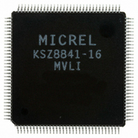
KSZ8841-16MVLI Micrel Inc, KSZ8841-16MVLI Datasheet - Page 52

KSZ8841-16MVLI
Manufacturer Part Number
KSZ8841-16MVLI
Description
Single Ethernet Port + Generic (8, 16-bit) Bus Interface( )
Manufacturer
Micrel Inc
Specifications of KSZ8841-16MVLI
Controller Type
Ethernet Controller, MAC
Interface
Bus
Voltage - Supply
3.1 V ~ 3.5 V
Operating Temperature
-40°C ~ 85°C
Mounting Type
Surface Mount
Package / Case
128-LQFP
Operating Supply Voltage (typ)
3.3V
Operating Temperature Classification
Industrial
Mounting
Surface Mount
Pin Count
128
Lead Free Status / RoHS Status
Lead free / RoHS Compliant
For Use With
576-1632 - BOARD EVALUATION KSZ8841-16MVL
Current - Supply
-
Lead Free Status / RoHS Status
Compliant, Lead free / RoHS Compliant
Other names
576-2114
KSZ8841-16MVLI
KSZ8841-16MVLI
Available stocks
Company
Part Number
Manufacturer
Quantity
Price
Company:
Part Number:
KSZ8841-16MVLI
Manufacturer:
MICREL
Quantity:
441
Register Map: MAC and PHY
Do not write to bit values or to registers defined as Reserved. Manipulating reserved bits or registers causes
unpredictable and often fatal results. If the user wants to write to these reserved bits, the user has to read back these
reserved bits (RO or RW) first, then “OR” with the read value of the reserved bits and write back to these reserved bits.
Bit Type Definition
RO = Read only.
RW = Read/Write.
W1C = Write 1 to Clear (writing a one to this bit clears it).
Bank 0-63 Bank Select Register (0x0E): BSR (same location in all Banks)
The bank select register is used to select or to switch between different sets of register banks for I/O access.
There are a total of 64 banks available to select, including the built-in switch engine registers.
Bank 0 Base Address Register (0x00): BAR
This register holds the base address for decoding a device access. Its value is loaded from the external EEPROM (0x0H)
upon a power-on reset if the EEPROM Enable (EEEN) pin is tied to High. Its value can also be modified after reset.
Writing to this register does not store the value into the EEPROM. When the EEEN pin is tied to Low, the default base
address is 0x300.
October 2007
Micrel, Inc.
Bit
15-6
5-0
Bit
15-8
7-5
4-0
0x03 if EEEN
is Low or, the
value from
EEPROM if
EEEN is High
0x00 if EEEN
is Low or, the
value from
EEPROM if
EEEN is High
Default Value
0x000
0x00
Default Value
0x00
R/W
RO
R/W
R/W
RW
RW
RO
Description
Reserved
BSA Bank Select Address Bits
BSA bits select the I/O register bank in use.
This register is always accessible regardless of the register bank currently selected.
Notes:
The bank select register can be accessed as a doubleword (32-bit) at offset 0xC, as a word
(16-bit) at offset 0xE, or as a byte (8-bit) at offset 0xE.
A doubleword write to offset 0xC writes to the BANK Select Register but does not write to
registers 0xC and 0xD; it only writes to register 0xE.
Description
BARH Base Address High
These bits are compared against the address on the bus ADDR[15:8] to determine the
BASE for the KSZ8841M registers.
BARL Base Address Low
These bits are compared against the address on the bus ADDR[7:5] to determine the BASE
for the KSZ8841M registers.
Reserved
52
KSZ8841-16/32 MQL/MVL/MBL
M9999-102207-1.6


