SSM6L35FE(TE85L,F) Toshiba, SSM6L35FE(TE85L,F) Datasheet
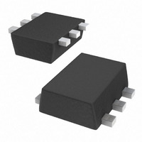
MOSFET N-CH/P-CH 20V .18A ES6

SSM6L35FE(TE85L,F)

Manufacturer Part Number
SSM6L35FE(TE85L,F)
Description
MOSFET N-CH/P-CH 20V .18A ES6
Manufacturer
Toshiba
Datasheet

Specifications of SSM6L35FE(TE85L,F)

Fet Type
N and P-Channel
Fet Feature
Logic Level Gate
Rds On (max) @ Id, Vgs
3 Ohm @ 50mA, 4V
Drain To Source Voltage (vdss)
20V
Current - Continuous Drain (id) @ 25° C
180mA, 100mA
Vgs(th) (max) @ Id
1V @ 1mA
Input Capacitance (ciss) @ Vds
9.5pF @ 3V
Power - Max
150mW
Mounting Type
Surface Mount
Package / Case
ES6
Lead Free Status / RoHS Status
Lead free / RoHS Compliant
Gate Charge (qg) @ Vgs
-
Other names
SSM6L35FE(TE85LF)TR
○ High-Speed Switching Applications
○ Analog Switch Applications
Q1
Q2
Absolute Maximum Ratings (Ta = 25 °C) (Common to the Q1, Q2)
Note: Using continuously under heavy loads (e.g. the application of high temperature/current/voltage and the
Note 1: Total rating
N-ch: 1.2-V drive
P-ch: 1.2-V drive
N-ch, P-ch, 2-in-1
Low ON-resistance Q1 N-ch: R
Drain–source voltage
Gate–source voltage
Drain current
Drain–source voltage
Gate–source voltage
Drain current
Drain power dissipation
Channel temperature
Storage temperature range
Absolute Maximum Ratings (Ta = 25°C)
significant change in temperature, etc.) may cause this product to decrease in the reliability significantly even if
the operating conditions (i.e. operating temperature/current/voltage, etc.) are within the absolute maximum
ratings.
Please design the appropriate reliability upon reviewing the Toshiba Semiconductor Reliability Handbook
(“Handling Precautions”/“Derating Concept and Methods”) and individual reliability data (i.e. reliability test report
and estimated failure rate, etc).
Mounted on an FR4 board
(25.4 mm × 25.4 mm × 1.6 mm, Cu Pad: 0.135 mm
Characteristics
Characteristics
Characteristic
TOSHIBA Field-Effect Transistor Silicon N / P Channel MOS Type
Q2 P-ch: R
Pulse
Pulse
DC
DC
: R
: R
: R
: R
: R
: R
on
on
on
on
on
on
on
on
= 44 Ω (max) (@V
= 20 Ω (max) (@V
= 8 Ω (max) (@V
= 4 Ω (max) (@V
= 3 Ω (max) (@V
= 22 Ω (max) (@V
= 11 Ω (max) (@V
= 8 Ω (max) (@V
SSM6L35FE
P
D
Symbol
Symbol
Symbol
V
V
V
V
(Note 1)
T
I
I
T
GSS
GSS
DSS
DSS
I
DP
I
DP
stg
D
D
ch
−55 to 150
GS
Rating
Rating
GS
Rating
GS
GS
GS
GS
GS
GS
-100
-200
±10
180
360
±10
150
150
-20
20
1
= -1.2 V)
= -2.5 V)
= 1.2 V)
= -1.5 V)
= 1.5 V)
= 2.5 V)
= 4.0 V)
= -4.0 V)
2
× 6)
Unit
Unit
Unit
mW
mA
mA
°C
°C
V
V
V
V
Weight: 3.0 mg (typ.)
JEDEC
JEITA
TOSHIBA
ES6
1
2
3
1.Source1 4.Source2
2.Gate1
3.Drain2
1.2±0.05
1.6±0.05
SSM6L35FE
2-2N1D
2008-03-21
-
-
5.Gate2
6.Drain1
Unit: mm
6
5
4

Related parts for SSM6L35FE(TE85L,F)

SSM6L35FE(TE85L,F) Summary of contents

Page 1

... Please design the appropriate reliability upon reviewing the Toshiba Semiconductor Reliability Handbook (“Handling Precautions”/“Derating Concept and Methods”) and individual reliability data (i.e. reliability test report and estimated failure rate, etc) ...

Page 2

Q1 Electrical Characteristics Characteristics Gate leakage current Drain–source breakdown voltage Drain cutoff current Gate threshold voltage Forward transfer admittance Drain–source ON-resistance Input capacitance Reverse transfer capacitance Output capacitance Turn-on time Switching time Turn-off time Drain–source forward voltage Q2 Electrical Characteristics ...

Page 3

Q1 Switching Time Test Circuit (a) Test Circuit 2 μ D.U. ≤ 1% < Ω) (Z out Common Source ...

Page 4

Q1 (N-ch MOSFET) I – 400 2.5 V 300 200 100 0 0 0.5 1 Drain–source voltage V R – (ON Gate–source voltage ...

Page 5

Q1 (N-ch MOSFET) V – 1.0 0.5 0 − Ambient temperature Ta (°C) I – 1000 Common Source 100 25° ...

Page 6

Q2 (P-ch MOSFET) I – -250 -10V -200 -150 -100 - -0.5 -1 Drain–source voltage (ON Gate–source voltage (ON ...

Page 7

Q2 (P-ch MOSFET) V – -0.8 -0.6 -0.4 -0.2 0 − Ambient temperature Ta (°C) I – 1000 Common Source 100 ...

Page 8

... Product shall not be used for or incorporated into any products or systems whose manufacture, use, or sale is prohibited under any applicable laws or regulations. • The information contained herein is presented only as guidance for Product use. No responsibility is assumed by TOSHIBA for any infringement of patents or any other intellectual property rights of third parties that may result from the use of Product. No license to any intellectual property right is granted by this document, whether express or implied, by estoppel or otherwise. • ...

Related keywords