NTLJD3119CTAG ON Semiconductor, NTLJD3119CTAG Datasheet - Page 2
NTLJD3119CTAG
Manufacturer Part Number
NTLJD3119CTAG
Description
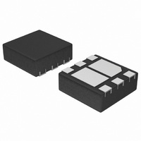
MOSFET N/P-CH 20V 4.6/4.1A 6WDFN
Manufacturer
ON Semiconductor
Datasheet
1.NTLJD3119CTAG.pdf
(10 pages)
Specifications of NTLJD3119CTAG
Fet Type
N and P-Channel
Fet Feature
Logic Level Gate
Rds On (max) @ Id, Vgs
65 mOhm @ 3.8A, 4.5V
Drain To Source Voltage (vdss)
20V
Current - Continuous Drain (id) @ 25° C
2.6A, 2.3A
Vgs(th) (max) @ Id
1V @ 250µA
Gate Charge (qg) @ Vgs
3.7nC @ 4.5V
Input Capacitance (ciss) @ Vds
271pF @ 10V
Power - Max
710mW
Mounting Type
Surface Mount
Package / Case
6-VDFN Exposed Pad
Configuration
Dual
Transistor Polarity
N and P-Channel
Resistance Drain-source Rds (on)
0.065 Ohm @ 4.5 V @ N Channel
Forward Transconductance Gfs (max / Min)
4.2 S, 3.1 S
Drain-source Breakdown Voltage
20 V
Gate-source Breakdown Voltage
+/- 8 V
Continuous Drain Current
3.8 A @ N Channel or 3.3 A @ P Channel
Power Dissipation
1500 mW
Maximum Operating Temperature
+ 150 C
Mounting Style
SMD/SMT
Minimum Operating Temperature
- 55 C
Lead Free Status / RoHS Status
Lead free / RoHS Compliant
Available stocks
Company
Part Number
Manufacturer
Quantity
Price
Company:

Part Number:
NTLJD3119CTAG
Manufacturer:
ON
Quantity:
2 976


3. Surface Mounted on FR4 Board using 1 in sq pad size (Cu area = 1.127 in sq [2 oz] including traces).
4. Surface Mounted on FR4 Board using the minimum recommended pad size (30 mm
THERMAL RESISTANCE RATINGS
SINGLE OPERATION (SELF−HEATED)
DUAL OPERATION (EQUALLY HEATED)
Junction−to−Ambient – Steady State (Note 3)
Junction−to−Ambient – Steady State Min Pad (Note 4)
Junction−to−Ambient – t ≤ 5 s (Note 3)
Junction−to−Ambient – Steady State (Note 3)
Junction−to−Ambient – Steady State Min Pad (Note 4)
Junction−to−Ambient – t ≤ 5 s (Note 3)
Parameter
http://onsemi.com
2
2
, 2 oz Cu).
Symbol
R
R
R
R
R
R
qJA
qJA
qJA
qJA
qJA
qJA
Max
177
133
83
54
58
40
°C/W
°C/W
Unit
Related parts for NTLJD3119CTAG
Image
Part Number
Description
Manufacturer
Datasheet
Request
R

Part Number:
Description:
ON Semiconductor [VOLTAGE REGULATOR]
Manufacturer:
ON Semiconductor
Datasheet:
Part Number:
Description:
357-036-542-201 CARDEDGE 36POS DL .156 BLK LOPRO
Manufacturer:
ON Semiconductor
Datasheet:
Part Number:
Description:
357-036-542-201 CARDEDGE 36POS DL .156 BLK LOPRO
Manufacturer:
ON Semiconductor
Datasheet:
Part Number:
Description:
357-036-542-201 CARDEDGE 36POS DL .156 BLK LOPRO
Manufacturer:
ON Semiconductor
Datasheet:
Part Number:
Description:
357-036-542-201 CARDEDGE 36POS DL .156 BLK LOPRO
Manufacturer:
ON Semiconductor
Datasheet:
Part Number:
Description:
357-036-542-201 CARDEDGE 36POS DL .156 BLK LOPRO
Manufacturer:
ON Semiconductor
Datasheet:
Part Number:
Description:
357-036-542-201 CARDEDGE 36POS DL .156 BLK LOPRO
Manufacturer:
ON Semiconductor
Datasheet:
Part Number:
Description:
357-036-542-201 CARDEDGE 36POS DL .156 BLK LOPRO
Manufacturer:
ON Semiconductor
Datasheet:
Part Number:
Description:
357-036-542-201 CARDEDGE 36POS DL .156 BLK LOPRO
Manufacturer:
ON Semiconductor
Datasheet:
Part Number:
Description:
357-036-542-201 CARDEDGE 36POS DL .156 BLK LOPRO
Manufacturer:
ON Semiconductor
Datasheet:
Part Number:
Description:
357-036-542-201 CARDEDGE 36POS DL .156 BLK LOPRO
Manufacturer:
ON Semiconductor
Datasheet:
Part Number:
Description:
Manufacturer:
ON Semiconductor
Datasheet:
Part Number:
Description:
Manufacturer:
ON Semiconductor
Datasheet:
Part Number:
Description:
Manufacturer:
ON Semiconductor
Datasheet: