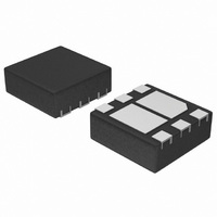
NTLJD3119CTAG ON Semiconductor, NTLJD3119CTAG Datasheet - Page 9

NTLJD3119CTAG
Manufacturer Part Number
NTLJD3119CTAG
Description
MOSFET N/P-CH 20V 4.6/4.1A 6WDFN
Manufacturer
ON Semiconductor
Datasheet
1.NTLJD3119CTAG.pdf
(10 pages)
Specifications of NTLJD3119CTAG
Fet Type
N and P-Channel
Fet Feature
Logic Level Gate
Rds On (max) @ Id, Vgs
65 mOhm @ 3.8A, 4.5V
Drain To Source Voltage (vdss)
20V
Current - Continuous Drain (id) @ 25° C
2.6A, 2.3A
Vgs(th) (max) @ Id
1V @ 250µA
Gate Charge (qg) @ Vgs
3.7nC @ 4.5V
Input Capacitance (ciss) @ Vds
271pF @ 10V
Power - Max
710mW
Mounting Type
Surface Mount
Package / Case
6-VDFN Exposed Pad
Configuration
Dual
Transistor Polarity
N and P-Channel
Resistance Drain-source Rds (on)
0.065 Ohm @ 4.5 V @ N Channel
Forward Transconductance Gfs (max / Min)
4.2 S, 3.1 S
Drain-source Breakdown Voltage
20 V
Gate-source Breakdown Voltage
+/- 8 V
Continuous Drain Current
3.8 A @ N Channel or 3.3 A @ P Channel
Power Dissipation
1500 mW
Maximum Operating Temperature
+ 150 C
Mounting Style
SMD/SMT
Minimum Operating Temperature
- 55 C
Lead Free Status / RoHS Status
Lead free / RoHS Compliant
Available stocks
Company
Part Number
Manufacturer
Quantity
Price
Company:
Part Number:
NTLJD3119CTAG
Manufacturer:
ON
Quantity:
2 976
1000
100
0.000001
0.1
10
1
0.05
0.02
0.01
D = 0.5
0.2
0.1
0.00001
SINGLE PULSE
TYPICAL PERFORMANCE CURVES
0.0001
0.001
Figure 22. Thermal Response
http://onsemi.com
0.01
t, TIME (s)
9
P
(pk)
DUTY CYCLE, D = t
(T
t
J
1
0.1
= 25°C unless otherwise noted)
t
2
1
1
/t
2
D CURVES APPLY FOR POWER
PULSE TRAIN SHOWN
READ TIME AT t
T
J(pk)
− T
10
A
*See Note 2 on Page 1
= P
(pk)
1
R
qJA
100
(t)
1000


