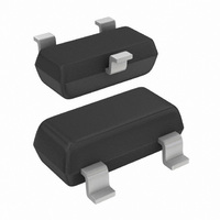
BSH112,235 NXP Semiconductors, BSH112,235 Datasheet - Page 2

BSH112,235
Manufacturer Part Number
BSH112,235
Description
MOSFET N-CH 60V 300MA SOT-23
Manufacturer
NXP Semiconductors
Series
TrenchMOS™r
Datasheet
1.BSH112235.pdf
(13 pages)
Specifications of BSH112,235
Package / Case
SOT-23-3, TO-236-3, Micro3™, SSD3, SST3
Fet Type
MOSFET N-Channel, Metal Oxide
Fet Feature
Logic Level Gate
Rds On (max) @ Id, Vgs
5 Ohm @ 500mA, 10V
Drain To Source Voltage (vdss)
60V
Current - Continuous Drain (id) @ 25° C
300mA
Vgs(th) (max) @ Id
2V @ 1mA
Input Capacitance (ciss) @ Vds
40pF @ 10V
Power - Max
830mW
Mounting Type
Surface Mount
Minimum Operating Temperature
- 65 C
Configuration
Single
Transistor Polarity
N-Channel
Resistance Drain-source Rds (on)
5 Ohm @ 10 V
Drain-source Breakdown Voltage
60 V
Gate-source Breakdown Voltage
+/- 15 V
Continuous Drain Current
0.3 A
Power Dissipation
830 mW
Maximum Operating Temperature
+ 150 C
Mounting Style
SMD/SMT
Lead Free Status / RoHS Status
Lead free / RoHS Compliant
Gate Charge (qg) @ Vgs
-
Lead Free Status / Rohs Status
Lead free / RoHS Compliant
Other names
568-1768-2
934056035235
BSH112 /T3
934056035235
BSH112 /T3
5. Quick reference data
Table 2:
6. Limiting values
Table 3:
In accordance with the Absolute Maximum Rating System (IEC 60134).
Philips Semiconductors
9397 750 07305
Product specification
Symbol Parameter
V
I
P
T
R
Symbol Parameter
V
V
V
I
I
P
T
T
Source-drain diode
I
I
D
D
DM
S
SM
j
stg
j
DS
tot
DS
DGR
GS
tot
DSon
drain-source voltage (DC)
drain current (DC)
total power dissipation
junction temperature
drain-source on-state resistance
drain-source voltage (DC)
drain-gate voltage (DC)
gate-source voltage (DC)
drain current (DC)
peak drain current
total power dissipation
storage temperature
operating junction temperature
source (diode forward) current (DC)
peak source (diode forward) current
Quick reference data
Limiting values
Rev. 01 — 25 August 2000
Conditions
T
T
T
V
V
Conditions
T
T
T
Figure 2
T
T
Figure 3
T
T
T
j
sp
sp
j
j
sp
sp
sp
sp
sp
sp
GS
GS
= 25 to 150 C
= 25 to 150 C
= 25 to 150 C; R
= 25 C; V
= 25 C
= 25 C; V
= 100 C; V
= 25 C; pulsed; t
= 25 C;
= 25 C
= 25 C; pulsed; t
= 10 V; I
= 4.5 V; I
and
N-channel enhancement mode field-effect transistor
Figure 1
D
3
D
GS
GS
= 500 mA
= 75 mA
GS
= 10 V
= 10 V;
= 10 V;
GS
p
p
= 20 k
10 s;
10 s
Figure 2
Typ
2.8
3.8
Min
65
65
© Philips Electronics N.V. 2000. All rights reserved.
Max
60
300
0.83
150
5
5.3
Max
60
60
300
190
1.2
0.83
+150
+150
300
1.2
BSH112
15
Unit
V
mA
W
Unit
V
V
V
mA
mA
A
W
mA
A
C
C
C
2 of 13


