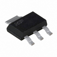
BSP250,135 NXP Semiconductors, BSP250,135 Datasheet - Page 9

BSP250,135
Manufacturer Part Number
BSP250,135
Description
MOSFET P-CH 30V 3A SOT223
Manufacturer
NXP Semiconductors
Datasheet
1.BSP250135.pdf
(12 pages)
Specifications of BSP250,135
Package / Case
SOT-223 (3 leads + Tab), SC-73, TO-261
Fet Type
MOSFET P-Channel, Metal Oxide
Fet Feature
Logic Level Gate
Rds On (max) @ Id, Vgs
250 mOhm @ 1A, 10V
Drain To Source Voltage (vdss)
30V
Current - Continuous Drain (id) @ 25° C
3A
Vgs(th) (max) @ Id
2.8V @ 1mA
Gate Charge (qg) @ Vgs
25nC @ 10V
Input Capacitance (ciss) @ Vds
250pF @ 20V
Power - Max
1.65W
Mounting Type
Surface Mount
Minimum Operating Temperature
- 65 C
Configuration
Single Dual Drain
Transistor Polarity
P-Channel
Resistance Drain-source Rds (on)
0.25 Ohm @ 10 V
Drain-source Breakdown Voltage
30 V
Gate-source Breakdown Voltage
+/- 20 V
Continuous Drain Current
3 A
Power Dissipation
1650 mW
Maximum Operating Temperature
+ 150 C
Mounting Style
SMD/SMT
Lead Free Status / RoHS Status
Lead free / RoHS Compliant
Lead Free Status / RoHS Status
Lead free / RoHS Compliant, Lead free / RoHS Compliant
Other names
934033450135
BSP250 /T3
BSP250 /T3
BSP250 /T3
BSP250 /T3
Philips Semiconductors
DEFINITIONS
LIFE SUPPORT APPLICATIONS
These products are not designed for use in life support appliances, devices, or systems where malfunction of these
products can reasonably be expected to result in personal injury. Philips customers using or selling these products for
use in such applications do so at their own risk and agree to fully indemnify Philips for any damages resulting from such
improper use or sale.
1997 Jun 20
Data Sheet Status
Objective specification
Preliminary specification
Product specification
Limiting values
Limiting values given are in accordance with the Absolute Maximum Rating System (IEC 134). Stress above one or
more of the limiting values may cause permanent damage to the device. These are stress ratings only and operation
of the device at these or at any other conditions above those given in the Characteristics sections of the specification
is not implied. Exposure to limiting values for extended periods may affect device reliability.
Application information
Where application information is given, it is advisory and does not form part of the specification.
P-channel enhancement mode
vertical D-MOS transistor
This data sheet contains target or goal specifications for product development.
This data sheet contains preliminary data; supplementary data may be published later.
This data sheet contains final product specifications.
9
Product specification
BSP250


