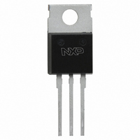
PSMN4R3-30PL,127 NXP Semiconductors, PSMN4R3-30PL,127 Datasheet - Page 8

PSMN4R3-30PL,127
Manufacturer Part Number
PSMN4R3-30PL,127
Description
MOSFET N-CH 30V 100A TO-220AB3
Manufacturer
NXP Semiconductors
Datasheet
1.PSMN4R3-30PL127.pdf
(13 pages)
Specifications of PSMN4R3-30PL,127
Package / Case
TO-220AB-3
Fet Type
MOSFET N-Channel, Metal Oxide
Fet Feature
Logic Level Gate
Rds On (max) @ Id, Vgs
4.3 mOhm @ 15A, 10V
Drain To Source Voltage (vdss)
30V
Current - Continuous Drain (id) @ 25° C
100A
Vgs(th) (max) @ Id
2.15V @ 1mA
Gate Charge (qg) @ Vgs
41.5nC @ 10V
Input Capacitance (ciss) @ Vds
2400pF @ 12V
Power - Max
103W
Mounting Type
Through Hole
Transistor Polarity
N-Channel
Resistance Drain-source Rds (on)
4.3 mOhms
Drain-source Breakdown Voltage
30 V
Continuous Drain Current
100 A
Power Dissipation
103 W
Mounting Style
Through Hole
Lead Free Status / RoHS Status
Lead free / RoHS Compliant
Lead Free Status / RoHS Status
Lead free / RoHS Compliant, Lead free / RoHS Compliant
Other names
568-4897-5
934063918127
934063918127
NXP Semiconductors
PSMN4R3-30PL_1
Product data sheet
Fig 11. Gate-source threshold voltage as a function of
Fig 13. Drain-source on-state resistance as a function
R
(mΩ)
V
DSon
GS (th)
(V)
16
12
3
2
1
0
8
4
0
-60
junction temperature
of drain current; typical values
0
20
0
3
40
max
min
typ
60
V
GS
60
3.5
(V) =10
120
4
80
003aad237
003a a c982
T
I
j
D
(°C)
(A)
4.5
5
180
100
Rev. 01 — 16 June 2009
Fig 12. Normalized drain-source on-state resistance
Fig 14. Gate charge waveform definitions
a
1.5
0.5
2
1
0
−60
factor as a function of junction temperature
N-channel 30 V 4.3 mΩ logic level MOSFET
V
V
V
V
GS(pl)
DS
GS(th)
GS
Q
0
GS1
I
Q
PSMN4R3-30PL
D
GS
Q
GS2
60
Q
G(tot)
Q
GD
120
© NXP B.V. 2009. All rights reserved.
003aaa508
T
j
( ° C)
03aa27
180
8 of 13


