IRF644NS Vishay, IRF644NS Datasheet - Page 3
IRF644NS
Manufacturer Part Number
IRF644NS
Description
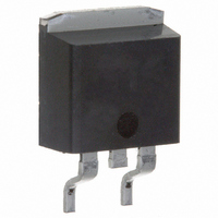
MOSFET N-CH 250V 14A D2PAK
Manufacturer
Vishay
Datasheet
1.IRF644NS.pdf
(8 pages)
Specifications of IRF644NS
Fet Type
MOSFET N-Channel, Metal Oxide
Fet Feature
Standard
Rds On (max) @ Id, Vgs
240 mOhm @ 8.4A, 10V
Drain To Source Voltage (vdss)
250V
Current - Continuous Drain (id) @ 25° C
14A
Vgs(th) (max) @ Id
4V @ 250µA
Gate Charge (qg) @ Vgs
54nC @ 10V
Input Capacitance (ciss) @ Vds
1060pF @ 25V
Power - Max
150W
Mounting Type
Surface Mount
Package / Case
D²Pak, TO-263 (2 leads + tab)
Lead Free Status / RoHS Status
Contains lead / RoHS non-compliant
Other names
*IRF644NS
Available stocks
Company
Part Number
Manufacturer
Quantity
Price

Part Number:
IRF644NS
Manufacturer:
IR
Quantity:
20 000
Part Number:
IRF644NSPBF
Manufacturer:
IR
Quantity:
20 000


Notes
a. Repetitive rating; pulse width limited by maximum junction temperature (see fig. 11).
b. Pulse width ≤ 300 µs; duty cycle ≤ 2 %.
c. This is only applied to TO-220 package.
d. When mounted on 1" square PCB (fr-4 or G-10 material).
TYPICAL CHARACTERISTICS 25 °C, unless otherwise noted
Document Number: 91038
S-83000-Rev. A, 19-Jan-09
SPECIFICATIONS T
PARAMETER
Dynamic
Input Capacitance
Output Capacitance
Reverse Transfer Capacitance
Total Gate Charge
Gate-Source Charge
Gate-Drain Charge
Turn-On Delay Time
Rise Time
Turn-Off Delay Time
Fall Time
Internal Drain Inductance
Internal Source Inductance
Drain-Source Body Diode Characteristics
Continuous Source-Drain Diode Current
Pulsed Diode Forward Current
Body Diode Voltage
Body Diode Reverse Recovery Time
Body Diode Reverse Recovery Charge
Forward Turn-On Time
91038_01
10
0.1
10
1
2
0.1
Top
Bottom
Fig. 1 - Typical Output Characteristics
IRF644N, IRF644NS, IRF644NL, SiHF644N, SiHF644NS, SiHF644NL
V
DS
15 V
10 V
8.0 V
7.0 V
6.0 V
5.5 V
5.0 V
4.5 V
V
GS
, Drain-to-Source Voltage (V)
1
J
a
= 25 °C, unless otherwise noted
20 µs Pulse Width
T
10
C
=
25 °C
4.5 V
SYMBOL
t
t
C
C
C
Q
V
Q
d(on)
d(off)
I
Q
Q
L
L
t
SM
I
t
on
oss
t
t
rss
SD
iss
S
rr
gs
gd
r
D
S
f
g
rr
10
2
Between lead,
6 mm (0.25") from
package and center of
die contact
MOSFET symbol
showing the
integral reverse
p - n junction diode
T
V
R
J
Intrinsic turn-on time is negligible (turn-on is dominated by L
GS
= 25 °C, I
G
T
J
= 6.2 Ω, V
= 10 V
= 25 °C, I
V
f = 1.0 MHz, see fig. 5
DD
TEST CONDITIONS
= 125 V, I
F
91038_02
V
V
= 14 A, dI/dt = 100 A/µs
DS
GS
S
GS
= 14 A, V
I
D
= 25 V,
= 10 V, see fig. 10
= 0 V,
= 8.4 A, V
10
see fig. 6 and 13
0.1
10
1
D
2
0.1
= 8.4 A,
Fig. 2 - Typical Output Characteristics
Top
Bottom
GS
G
G
DS
= 0 V
V
DS ,
= 200 V,
15 V
10 V
8.0 V
7.0 V
6.0 V
5.5 V
5.0 V
4.5 V
V
GS
b
Drain-to-Source Voltage (V)
D
S
D
S
b
b
b
1
MIN.
-
-
-
-
-
-
-
-
-
-
-
-
-
-
-
-
-
Vishay Siliconix
20 µs Pulse Width
T
TYP.
1060
10
140
165
C
4.5
7.5
1.0
38
10
21
30
17
-
-
-
-
-
-
=
175 °C
www.vishay.com
MAX.
250
9.2
1.3
1.6
S
54
26
14
56
4.5 V
-
-
-
-
-
-
-
-
-
and L
10
UNIT
2
D
µC
pF
nC
nH
ns
ns
)
A
V
3
Related parts for IRF644NS
Image
Part Number
Description
Manufacturer
Datasheet
Request
R

Part Number:
Description:
MOSFET N-CH 250V 14A TO-220AB
Manufacturer:
Vishay
Datasheet:

Part Number:
Description:
357-036-542-201 CARDEDGE 36POS DL .156 BLK LOPRO
Manufacturer:
Vishay
Datasheet:
Part Number:
Description:
357-036-542-201 CARDEDGE 36POS DL .156 BLK LOPRO
Manufacturer:
Vishay
Datasheet:
Part Number:
Description:
357-036-542-201 CARDEDGE 36POS DL .156 BLK LOPRO
Manufacturer:
Vishay
Datasheet:
Part Number:
Description:
357-036-542-201 CARDEDGE 36POS DL .156 BLK LOPRO
Manufacturer:
Vishay
Datasheet:
Part Number:
Description:
357-036-542-201 CARDEDGE 36POS DL .156 BLK LOPRO
Manufacturer:
Vishay
Datasheet:
Part Number:
Description:
357-036-542-201 CARDEDGE 36POS DL .156 BLK LOPRO
Manufacturer:
Vishay
Datasheet:
Part Number:
Description:
357-036-542-201 CARDEDGE 36POS DL .156 BLK LOPRO
Manufacturer:
Vishay
Datasheet:
Part Number:
Description:
357-036-542-201 CARDEDGE 36POS DL .156 BLK LOPRO
Manufacturer:
Vishay
Datasheet:
Part Number:
Description:
357-036-542-201 CARDEDGE 36POS DL .156 BLK LOPRO
Manufacturer:
Vishay
Datasheet:
Part Number:
Description:
357-036-542-201 CARDEDGE 36POS DL .156 BLK LOPRO
Manufacturer:
Vishay
Datasheet:
Part Number:
Description:
357-036-542-201 CARDEDGE 36POS DL .156 BLK LOPRO
Manufacturer:
Vishay
Datasheet:
Part Number:
Description:
357-036-542-201 CARDEDGE 36POS DL .156 BLK LOPRO
Manufacturer:
Vishay
Datasheet:
Part Number:
Description:
357-036-542-201 CARDEDGE 36POS DL .156 BLK LOPRO
Manufacturer:
Vishay
Datasheet:
Part Number:
Description:
357-036-542-201 CARDEDGE 36POS DL .156 BLK LOPRO
Manufacturer:
Vishay
Datasheet: