VRF141 Microsemi Power Products Group, VRF141 Datasheet

MOSFET RF PWR N-CH 28V 150W M174

VRF141

Manufacturer Part Number
VRF141
Description
MOSFET RF PWR N-CH 28V 150W M174
Manufacturer
Microsemi Power Products Group
Datasheet

Specifications of VRF141

Transistor Type
N-Channel
Frequency
30MHz
Gain
20dB
Voltage - Rated
80V
Current Rating
20A
Current - Test
250mA
Voltage - Test
28V
Power - Output
150W
Package / Case
M174
Lead Free Status / RoHS Status
Lead free / RoHS Compliant
Noise Figure
-
Other names
VRF141MP
VRF141MP

Available stocks

Company
Part Number
Manufacturer
Quantity
Price
Part Number:
VRF141
Manufacturer:
Triquint
Quantity:
1 400
Part Number:
VRF141MP
Manufacturer:
MICROSEMI/美高森美
Quantity:
20 000
The VRF141 is a gold-metallized silicon n-channel RF power transistor de-
signed for broadband commercial and military applications requiring high power
and gain without compromising reliability, ruggedness, or inter-modulation
distortion.
Maximum Ratings
Static Electrical Characteristics
Thermal Characteristics
Dynamic Characteristics
FEATURES
• Improved Ruggedness V
• 150W with 22dB Typical Gain @ 30MHz, 28V
• 150W with 13dB Typical Gain @ 175MHz, 28V
• Excellent Stability & Low IMD
• Common Source Confi guration
Symbol
Symbol
Symbol
Symbol
V
RF POWER VERTICAL MOSFET
V
V
CAUTION: These Devices are Sensitive to Electrostatic Discharge. Proper Handling Procedures Should Be Followed.
R
(BR)DSS
C
V
T
C
DS(ON)
I
I
C
V
GS(TH)
GSS
g
P
DSS
T
I
θ JC
STG
DSS
oss
ISS
rss
D
GS
fs
D
J
Parameter
Drain-Source Breakdown Voltage (V
On State Drain Voltage (I
Zero Gate Voltage Drain Current (V
Gate-Source Leakage Current (V
Forward Transconductance (V
Gate Threshold Voltage (V
Characteristic
Junction to Case Thermal Resistance
Parameter
Drain-Source Voltage
Continuous Drain Current @ T
Gate-Source Voltage
Total Device dissipation @ T
Storage Temperature Range
Operating Junction Temperature
Parameter
Input Capacitance
Output Capacitance
Reverse Transfer Capacitance
(BR)DSS
= 80 V
D(ON)
DS
Microsemi Website - http://www.microsemi.com
C
= 10V, I
= 10A, V
= 25°C
DS
C
= 10V, I
= 25°C
DS
DS
= ±20V, V
GS
D
= 60V, V
GS
= 100mA)
= 0V, I
D
• 30:1 Load VSWR Capability at Specifi ed Operating Conditions
• Nitride Passivated
• Refractory Gold Metallization
• High Voltage Replacement for MRF141
• RoHS Compliant
= 10V)
= 5A)
D
DS
GS
= 100mA)
= 0V)
= 0V)
Test Conditions
V
f = 1MHz
V
All Ratings: T
DS
GS
= 28V
= 0V
C
=25°C unless otherwise specifi ed
Min
Min
Min
5.0
2.9
80
-65 to 150
VRF141
300
200
Typ
400
375
±40
Typ
Typ
0.9
50
80
20
3.6
28V, 150W, 175MHz
Max
Max
Max
0.60
VRF141
1.0
1.0
1.0
4.4
mhos
°C/W
Unit
Unit
Unit
Unit
mA
°C
μA
pF
W
V
V
A
V
V

Related parts for VRF141

VRF141 Summary of contents

Page 1

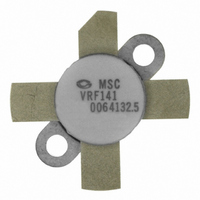
... RF POWER VERTICAL MOSFET The VRF141 is a gold-metallized silicon n-channel RF power transistor de- signed for broadband commercial and military applications requiring high power and gain without compromising reliability, ruggedness, or inter-modulation distortion. FEATURES • Improved Ruggedness (BR)DSS • 150W with 22dB Typical Gain @ 30MHz, 28V • ...

Page 2

... No Degradation in Output Power PEP Min Typ Max 23 -50 -75 250μs PULSE TEST<0.5 % DUTY CYCLE T = -55° 25° 125° DRAIN-TO-SOURCE VOLTAGE (V) DS FIGURE 2, Transfer Characteristics I DMax Pdmax R ds(on 125° 75° 100 V , DRAIN-TO-SOURCE VOLTAGE (V) DS FIGURE 4, Forward Safe Operating Area VRF141 Unit Unit dB ...

Page 3

... Vdd=28V, Idq = 250mA, Freq=175MHz 200 150 100 INPUT POWER (WATTS PEP) out Figure 7. P versus P IN Note Pulse Duration Duty Factor D = Peak θ 1.0 Vdd=28V, Idq = 250mA, Freq=30MHz INPUT POWER (WATTS PEP) out Figure 7. P versus P IN OUT 20 25 OUT VRF141 ...

Page 4

... MHz test Circuit 175 MHz test Circuit VRF141 ...

Page 5

... C 0.229 0.275 5.82 6.98 D 0.216 0.235 5.49 5.96 0.084 0.110 2.14 2. 0.144 0.178 3.66 4.52 J 0.003 0.007 0.08 0.17 K 0.435 11.0 M 45° NOM 45° NOM Q 0.115 0.130 2.93 3.30 R 0.246 0.255 6.25 6.47 U 0.720 0.730 18.29 18.54 VRF141 ...

Related keywords