APT1204R7KFLLG Microsemi Power Products Group, APT1204R7KFLLG Datasheet

MOSFET N-CH 1200V 3.5A TO-220

APT1204R7KFLLG

Manufacturer Part Number
APT1204R7KFLLG
Description
MOSFET N-CH 1200V 3.5A TO-220
Manufacturer
Microsemi Power Products Group
Series
POWER MOS 7®r
Datasheet

Specifications of APT1204R7KFLLG

Fet Type
MOSFET N-Channel, Metal Oxide
Fet Feature
Standard
Rds On (max) @ Id, Vgs
4.7 Ohm @ 1.75A, 10V
Drain To Source Voltage (vdss)
1200V (1.2kV)
Current - Continuous Drain (id) @ 25° C
3.5A
Vgs(th) (max) @ Id
5V @ 1mA
Gate Charge (qg) @ Vgs
31nC @ 10V
Input Capacitance (ciss) @ Vds
715pF @ 25V
Power - Max
135W
Mounting Type
Through Hole
Package / Case
TO-220
Lead Free Status / RoHS Status
Lead free / RoHS Compliant
STATIC ELECTRICAL CHARACTERISTICS
Power MOS 7
enhancement mode power MOSFETS. Both conduction and switching
losses are addressed with Power MOS 7
and Q
along with exceptionally fast switching speeds inherent with Microsemi's
patented metal gate structure.
• Lower Input Capacitance
• Lower Miller Capacitance
• Lower Gate Charge, Qg
MAXIMUM RATINGS
Symbol
Symbol
T
R
BV
V
V
V
J
I
V
E
E
DS(on)
I
GS(th)
,T
I
I
DSS
GSS
P
GSM
T
DSS
DM
I
AR
D
GS
AR
AS
DSS
D
L
STG
CAUTION: These Devices are Sensitive to Electrostatic Discharge. Proper Handling Procedures Should Be Followed.
g
. Power MOS 7
POWER MOS 7
Parameter
Drain-Source Voltage
Continuous Drain Current @ T
Pulsed Drain Current
Gate-Source Voltage Continuous
Gate-Source Voltage Transient
Total Power Dissipation @ T
Linear Derating Factor
Operating and Storage Junction Temperature Range
Lead Temperature: 0.063" from Case for 10 Sec.
Avalanche Current
Repetitive Avalanche Energy
Single Pulse Avalanche Energy
Characteristic / Test Conditions
Drain-Source Breakdown Voltage (V
Drain-Source On-State Resistance
Zero Gate Voltage Drain Current (V
Gate-Source Leakage Current (V
Gate Threshold Voltage (V
®
is a new generation of low loss, high voltage, N-Channel
®
combines lower conduction and switching losses
1
1
(Repetitive and Non-Repetitive)
• Increased Power Dissipation
• Easier To Drive
• TO-220 Package
DS
C
= V
C
= 25°C
1
Microsemi Website - http://www.microsemi.com
= 25°C
4
GS
GS
2
DS
, I
DS
®
= ±30V, V
GS
D
R
by significantly lowering R
(V
= 960V, V
= 1200V, V
= 1mA)
= 0V, I
GS
FREDFET
= 10V, I
D
DS
= 250µA)
GS
= 0V)
GS
= 0V, T
D
= 0V)
= 1.75A)
All Ratings: T
C
= 125°C)
DS(ON)
1200V 3.5A 4.700
C
= 25°C unless otherwise specified.
1200
MIN
3
APT1204R7KFLL
-55 to 150
G
D
1200
1.08
TYP
±30
±40
135
300
425
3.5
3.5
14
10
S
TO-220
±100
1000
MAX
4.70
250
5
G
Ohms
Amps
Watts
Amps
UNIT
Volts
Volts
W/°C
UNIT
Volts
Volts
mJ
µA
nA
°C
Ω Ω Ω Ω Ω
D
S

Related parts for APT1204R7KFLLG

APT1204R7KFLLG Summary of contents
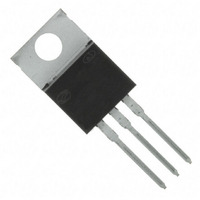
Page 1

POWER MOS 7 ® Power MOS new generation of low loss, high voltage, N-Channel enhancement mode power MOSFETS. Both conduction and switching losses are addressed with Power MOS 7 ® and Q . Power MOS 7 combines ...

Page 2

DYNAMIC CHARACTERISTICS Symbol Characteristic C Input Capacitance iss C Output Capacitance oss C Reverse Transfer Capacitance rss Q 3 Total Gate Charge g Q Gate-Source Charge gs Q Gate-Drain ("Miller ") Charge gd t Turn-on Delay Time d(on) t Rise ...

Page 3

0.386 Dissipated Power (Watts) 0.00336 Z are the external thermal EXT impedances: Case to sink, sink to ambient, etc. Set to zero when modeling only the case to junction. FIGURE 2, TRANSIENT THERMAL IMPEDANCE MODEL 10 ...

Page 4

OPERATION HERE 10 LIMITED (ON =+25° =+150°C SINGLE PULSE 0 100 V , DRAIN-TO-SOURCE VOLTAGE (VOLTS) DS FIGURE 10, MAXIMUM SAFE OPERATING AREA 3.5A D ...

Page 5

Typical Performance Curves Gate Voltage 10% t d(on) Drain Current 10% Drain Voltage Switching Energy Figure 18, Turn-on Switching Waveforms and Definitions APT15DQ120 APT60D120B D.U.T. Figure 20, Inductive ...

Related keywords