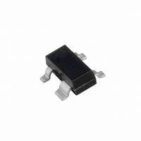
BF1100,215 NXP Semiconductors, BF1100,215 Datasheet - Page 4

BF1100,215
Manufacturer Part Number
BF1100,215
Description
MOSFET N-CH 14V 30MA SOT143
Manufacturer
NXP Semiconductors
Datasheet
1.BF1100215.pdf
(15 pages)
Specifications of BF1100,215
Package / Case
SOT-143, SOT-143B, TO-253AA
Transistor Type
N-Channel Dual Gate
Frequency
800MHz
Voltage - Rated
14V
Current Rating
30mA
Noise Figure
2dB
Current - Test
10mA
Voltage - Test
9V
Configuration
Single Dual Gate
Continuous Drain Current
0.03 A
Drain-source Breakdown Voltage
14 V
Gate-source Breakdown Voltage
13.2 V
Maximum Operating Temperature
+ 150 C
Minimum Operating Temperature
- 65 C
Mounting Style
SMD/SMT
Power Dissipation
200 mW @ Ta=50C
Transistor Polarity
N-Channel
Application
VHF/UHF
Channel Type
N
Channel Mode
Enhancement
Drain Source Voltage (max)
14V
Noise Figure (max)
2.8dB
Frequency (max)
1GHz
Package Type
SOT
Pin Count
3 +Tab
Input Capacitance (typ)@vds
2.2@9V@Gate 1/2.2@12V@Gate 1/1.6@9V@Gate 2/1.4@12V@Gate 2pF
Output Capacitance (typ)@vds
1.4@9V/1.1@12VpF
Reverse Capacitance (typ)
0.025@9V/0.025@12VpF
Operating Temp Range
-65C to 150C
Mounting
Surface Mount
Number Of Elements
2
Power Dissipation (max)
200@Ta=50CmW
Screening Level
Military
Lead Free Status / RoHS Status
Lead free / RoHS Compliant
Power - Output
-
Gain
-
Lead Free Status / Rohs Status
Lead free / RoHS Compliant
Other names
934036550215
BF1100 T/R
BF1100 T/R
BF1100 T/R
BF1100 T/R
NXP Semiconductors
THERMAL CHARACTERISTICS
Notes
1. Device mounted on a printed-circuit board.
2. T
STATIC CHARACTERISTICS
T
Notes
1. R
2. R
R
R
V
V
V
V
V
V
I
I
I
j
DSX
G1-SS
G2-SS
SYMBOL
SYMBOL
= 25 C; unless otherwise specified.
(BR)G1-SS
(BR)G2-SS
(F)S-G1
(F)S-G2
G1-S(th)
G2-S(th)
th j-a
th j-s
Dual-gate MOS-FETs
s
G1
G1
is the temperature at the soldering point of the source lead.
connects gate 1 to V
connects gate 1 to V
thermal resistance from junction to ambient
thermal resistance from junction to soldering point
gate 1-source breakdown voltage
gate 2-source breakdown voltage
forward source-gate 1 voltage
forward source-gate 2 voltage
gate 1-source threshold voltage
gate 2-source threshold voltage
drain-source current
gate 1 cut-off current
gate 2 cut-off current
BF1100
BF1100R
BF1100
BF1100R
PARAMETER
GG
GG
= 9 V; see Fig.27.
= 12 V; see Fig.27.
PARAMETER
Rev. 02 - 13 November 2007
V
V
V
V
V
I
V
I
V
I
V
I
V
R
V
R
V
V
D
D
D
D
G2-S
G1-S
G2-S
G1-S
G2-S
G2-S
G1-S
G1-S
G2-S
G2-S
G2-S
G1-S
G1
G1
= 20 A
= 20 A
= 20 A
= 20 A
= 180 k ; note 1
= 250 k ; note 2
= V
= V
= V
= V
= 4 V; V
= 4 V; V
= 4 V; V
= 4 V; V
= 4 V; V
= 4 V; V
= V
= V
CONDITIONS
DS
DS
DS
DS
DS
DS
= 0; I
= 0; I
= 0; I
= 0; I
= 0; V
= 0; V
DS
DS
DS
DS
DS
DS
note 1
note 2
T
T
= 9 V;
= 12 V;
= 9 V;
= 12 V;
= 9 V;
= 12 V;
s
s
CONDITIONS
S-G2
G1-S
G2-S
S-G1
G1-S
G2-S
= 92 C
= 78 C
= 10 mA
= 1 mA
= 1 mA
= 10 mA
= 12 V
= 12 V
13.2
13.2
0.5
0.5
0.3
0.3
0.3
0.3
8
8
BF1100; BF1100R
MIN.
VALUE
500
550
290
360
Product specification
20
20
1.5
1.5
1
1
1.2
1.2
13
13
50
50
MAX.
4 of 15
UNIT
K/W
K/W
K/W
K/W
V
V
V
V
V
V
V
V
mA
mA
nA
nA
UNIT


