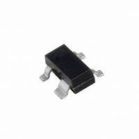
BF1100,215 NXP Semiconductors, BF1100,215 Datasheet - Page 9

BF1100,215
Manufacturer Part Number
BF1100,215
Description
MOSFET N-CH 14V 30MA SOT143
Manufacturer
NXP Semiconductors
Datasheet
1.BF1100215.pdf
(15 pages)
Specifications of BF1100,215
Package / Case
SOT-143, SOT-143B, TO-253AA
Transistor Type
N-Channel Dual Gate
Frequency
800MHz
Voltage - Rated
14V
Current Rating
30mA
Noise Figure
2dB
Current - Test
10mA
Voltage - Test
9V
Configuration
Single Dual Gate
Continuous Drain Current
0.03 A
Drain-source Breakdown Voltage
14 V
Gate-source Breakdown Voltage
13.2 V
Maximum Operating Temperature
+ 150 C
Minimum Operating Temperature
- 65 C
Mounting Style
SMD/SMT
Power Dissipation
200 mW @ Ta=50C
Transistor Polarity
N-Channel
Application
VHF/UHF
Channel Type
N
Channel Mode
Enhancement
Drain Source Voltage (max)
14V
Noise Figure (max)
2.8dB
Frequency (max)
1GHz
Package Type
SOT
Pin Count
3 +Tab
Input Capacitance (typ)@vds
2.2@9V@Gate 1/2.2@12V@Gate 1/1.6@9V@Gate 2/1.4@12V@Gate 2pF
Output Capacitance (typ)@vds
1.4@9V/1.1@12VpF
Reverse Capacitance (typ)
0.025@9V/0.025@12VpF
Operating Temp Range
-65C to 150C
Mounting
Surface Mount
Number Of Elements
2
Power Dissipation (max)
200@Ta=50CmW
Screening Level
Military
Lead Free Status / RoHS Status
Lead free / RoHS Compliant
Power - Output
-
Gain
-
Lead Free Status / Rohs Status
Lead free / RoHS Compliant
Other names
934036550215
BF1100 T/R
BF1100 T/R
BF1100 T/R
BF1100 T/R
NXP Semiconductors
handbook, halfpage
Dual-gate MOS-FETs
V
I
V
I
D
D
(mS)
DS
DS
Fig.21 Forward transfer admittance and phase as
(mS)
y fs
= 10 mA; T
= 10 mA; T
y is
10
10
10
10
= 9 V; V
= 9 V; V
10
1
1
2
2
1
10
Fig.19 Input admittance as a function of
10
a function of frequency; typical values.
G2
G2
amb
amb
= 4 V.
= 4 V.
= 25 C.
= 25 C.
frequency; typical values.
10
10
2
2
y fs
b is
g is
fs
f (MHz)
f (MHz)
MLD174
MLD172
10
10
Rev. 02 - 13 November 2007
3
3
10
10
1
(deg)
2
fs
handbook, halfpage
V
I
V
I
D
D
Fig.20 Reverse transfer admittance and phase as
( S)
DS
DS
(mS)
y rs
= 10 mA; T
=10 mA; T
y os
10
10
10
10
10
= 9 V; V
= 9 V; V
10
1
1
3
2
Fig.22 Output admittance as a function of
1
2
10
10
a function of frequency; typical values.
G2
G2
amb
amb
= 4 V.
= 4 V.
= 25 C.
frequency; typical values.
= 25 C.
BF1100; BF1100R
10
10
2
2
y rs
b os
g os
rs
f (MHz)
f (MHz)
Product specification
MLD173
MLD175
10
9 of 15
10
3
3
10
10
10
1
(deg)
rs
3
2


