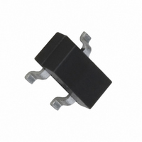
BF510,215 NXP Semiconductors, BF510,215 Datasheet - Page 2

BF510,215
Manufacturer Part Number
BF510,215
Description
MOSFET N-CH 20V 10MA SOT23
Manufacturer
NXP Semiconductors
Datasheet
1.BF510215.pdf
(9 pages)
Specifications of BF510,215
Package / Case
SST3 (SOT-23-3)
Current Rating
30mA
Frequency
100MHz
Transistor Type
N-Channel JFET
Noise Figure
1.5dB
Current - Test
5mA
Voltage - Test
10V
Configuration
Single
Mounting Style
SMD/SMT
Transistor Polarity
N-Channel
Forward Transconductance Gfs (max / Min)
0.0001 S
Drain Source Voltage Vds
20 V
Gate-source Cutoff Voltage
0.8 V
Maximum Drain Gate Voltage
20 V
Continuous Drain Current
30 mA
Drain Current (idss At Vgs=0)
3 mA
Power Dissipation
250 mW
Maximum Operating Temperature
+ 150 C
Channel Type
N
Drain Current (max)
30mA
Drain-gate Voltage (max)
20V
Drain-source Volt (max)
20V
Operating Temperature (max)
150C
Operating Temperature Classification
Military
Mounting
Surface Mount
Pin Count
3
Lead Free Status / RoHS Status
Lead free / RoHS Compliant
Power - Output
-
Gain
-
Lead Free Status / Rohs Status
Compliant
Other names
933505270215::BF510 T/R::BF510 T/R
NXP Semiconductors
DESCRIPTION
Asymmetrical N-channel planar
epitaxial junction field-effect
transistors in the miniature plastic
envelope intended for applications up
to the v.h.f. range in hybrid thick and
thin-film circuits. Special features are
the low feedback capacitance and the
low noise figure. These features
make the product very suitable for
applications such as the r.f. stages in
f.m. portables (BF510), car radios
(BF511) and mains radios (BF512) or
the mixer stage (BF513).
PINNING - SOT23
QUICK REFERENCE DATA
December 1997
1
2
3
Drain-source voltage
Drain current (DC or average)
Total power dissipation
Drain current
Transfer admittance (common source)
Feedback capacitance
Noise figure at optimum source admittance
N-channel silicon field-effect transistors
up to T
V
V
V
V
G
V
V
= gate
= drain
= source
DS
DS
DS
DS
DS
DS
S
= 1 mS; B
= 10 V; V
= 10 V; V
= 10 V; V
= 10 V; I
= 10 V; V
= 10 V; I
amb
= 40 C
D
D
GS
GS
GS
GS
= 5 mA
S
= 5 mA
= 3 mS; f = 100 MHz
= 0
= 0; f = 1 kHz
= 0
= 0
MARKING CODE
BF510 = S6p
BF511 = S7p
BF512 = S8p
BF513 = S9p
handbook, halfpage
V
I
P
I
y
C
C
F
F
D
DSS
DS
tot
rs
rs
fs
2
Fig.1 Simplified outline and symbol.
Top view
max.
max.
max.
typ.
typ.
typ.
typ.
1
BF510
3
0.7
3.0
2.5
0.3
1.5
2
511
2.5
7.0
0.3
1.5
4
250
g
20
30
MAM385
512
0.3
1.5
BF510 to 513
12
Product specification
d
s
6
6
513
0.3 pF
1.5 dB
10 mA
18 mA
7 mS
pF
dB
V
mA
mW


