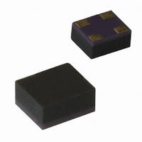
ATF-551M4-TR1 Avago Technologies US Inc., ATF-551M4-TR1 Datasheet - Page 18

ATF-551M4-TR1
Manufacturer Part Number
ATF-551M4-TR1
Description
IC TRANS E-PHEMT GAAS MINIPAK
Manufacturer
Avago Technologies US Inc.
Datasheet
1.ATF-551M4-TR2.pdf
(23 pages)
Specifications of ATF-551M4-TR1
Gain
17.5dB
Mfg Application Notes
ATF-541M4 AppNote
Transistor Type
pHEMT FET
Frequency
2GHz
Voltage - Rated
5V
Current Rating
100mA
Noise Figure
0.5dB
Current - Test
10mA
Voltage - Test
2.7V
Power - Output
14.6dBm
Package / Case
4-MiniPak (1412)
Power Dissipation Pd
270mW
Rf Transistor Case
MiniPak
Frequency Max
10GHz
Noise Figure Typ
0.5dB
Frequency Min
450MHz
Continuous Drain Current Id
0.1µA
Drain Current Idss Max
10mA
Drain Source Voltage Vds
2.7V
Rohs Compliant
Yes
Lead Free Status / RoHS Status
Lead free / RoHS Compliant
Other names
516-1509-2
Available stocks
Company
Part Number
Manufacturer
Quantity
Price
Company:
Part Number:
ATF-551M4-TR1
Manufacturer:
AVAGO
Quantity:
120 000
Part Number:
ATF-551M4-TR1
Manufacturer:
AVAGO/安华高
Quantity:
20 000
Company:
Part Number:
ATF-551M4-TR1G
Manufacturer:
AVAGO
Quantity:
140 000
S and Noise Parameter Measurements
The position of the reference planes used for the mea-
surement of both S and Noise Parameter measure-
ments is shown in Figure 36. The reference plane can be
described as being at the center of both the gate and
drain pads.
S and noise parameters are measured with a 50 ohm
microstrip test fixture made with a 0.010" thickness
aluminum substrate. Both source pads are connected
directly to ground via a 0.010" thickness metal rib
which provides a very low inductance path to ground
for both source pads. The inductance associated with
the addition of printed circuit board plated through
holes and source bypass capacitors must be added
to the computer circuit simulation to properly model
the effect of grounding the source leads in a typical
amplifier design.
Source
Figure . Position of the Reference Planes.
Noise Parameter Applications Information
The Fmin values are based on a set of 16 noise figure
measurements made at 16 different impedances using
an ATN NP5 test system. From these measurements,
a true Fmin is calculated. Fmin represents the true
minimum noise figure of the device when the device is
presented with an impedance matching network that
transforms the source impedance, typically 50Ω, to an
impedance represented by the reflection coefficient Γ
The designer must design a matching network that will
1
Pin 3
Pin 2
Gate
Reference
Plane
Microstrip
Transmission Lines
Vx
Drain
Pin 4
Source
Pin 1
o
.
present Γ
losses. The noise figure of the completed amplifier is
equal to the noise figure of the device plus the losses of
the matching network preceding the device. The noise
figure of the device is equal to Fmin only when the
device is presented with Γ
of the matching network is other than Γ
figure of the device will be greater than Fmin based on
the following equation.
NF = F
Where Rn/Zo is the normalized noise resistance, Γ
the optimum reflection coefficient required to produce
Fmin and Γ
impedance actually presented to the device.
The losses of the matching networks are non-zero
and they will also add to the noise figure of the device
creating a higher amplifier noise figure. The losses of
the matching networks are related to the Q of the com-
ponents and associated printed circuit board loss. Γ
typically fairly low at higher frequencies and increases
as frequency is lowered. Larger gate width devices
will typically have a lower Γ
gate width devices. Typically for FETs , the higher Γ
usually infers that an impedance much higher than
50Ω is required for the device to produce Fmin. At VHF
frequencies and even lower L Band frequencies, the
required impedance can be in the vicinity of several
thousand ohms. Matching to such a high impedance
requires very hi-Q components in order to minimize
circuit losses. As an example at 900 MHz, when air
wound coils (Q>100)are used for matching networks,
the loss can still be up to 0.25 dB which will add directly
to the noise figure of the device. Using muiltilayer
molded inductors with Qs in the 30 to 50 range results
in additional loss over the air wound coil. Losses as high
as 0.5 dB or greater add to the typical 0.15 dB Fmin of
the device creating an amplifier noise figure of nearly
0.65 dB.
min
+ 4 R
o
Zo (|1 + Γ
to the device with minimal associated circuit
s
n
is the reflection coefficient of the source
|Γ
s
o
– Γ
|
2
)(1 - |Γ
o
|
2
o
. If the reflection coefficient
o
s
|
as compared to narrower
2
)
o
, then the noise
o
o
is
is
o


