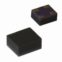
ATF-551M4-TR1 Avago Technologies US Inc., ATF-551M4-TR1 Datasheet - Page 2

ATF-551M4-TR1
Manufacturer Part Number
ATF-551M4-TR1
Description
IC TRANS E-PHEMT GAAS MINIPAK
Manufacturer
Avago Technologies US Inc.
Datasheet
1.ATF-551M4-TR2.pdf
(23 pages)
Specifications of ATF-551M4-TR1
Gain
17.5dB
Mfg Application Notes
ATF-541M4 AppNote
Transistor Type
pHEMT FET
Frequency
2GHz
Voltage - Rated
5V
Current Rating
100mA
Noise Figure
0.5dB
Current - Test
10mA
Voltage - Test
2.7V
Power - Output
14.6dBm
Package / Case
4-MiniPak (1412)
Power Dissipation Pd
270mW
Rf Transistor Case
MiniPak
Frequency Max
10GHz
Noise Figure Typ
0.5dB
Frequency Min
450MHz
Continuous Drain Current Id
0.1µA
Drain Current Idss Max
10mA
Drain Source Voltage Vds
2.7V
Rohs Compliant
Yes
Lead Free Status / RoHS Status
Lead free / RoHS Compliant
Other names
516-1509-2
Available stocks
Company
Part Number
Manufacturer
Quantity
Price
Company:
Part Number:
ATF-551M4-TR1
Manufacturer:
AVAGO
Quantity:
120 000
Part Number:
ATF-551M4-TR1
Manufacturer:
AVAGO/安华高
Quantity:
20 000
Company:
Part Number:
ATF-551M4-TR1G
Manufacturer:
AVAGO
Quantity:
140 000
ATF-551M4 Absolute Maximum Ratings
Notes:
1. Operation of this device above any one of these parameters may
2. Assumes DC quiescent conditions.
3. Source lead temperature is 25°C. Derate 6 mW/°C for T
4. Thermal resistance measured using 150°C Liquid Crystal Measure-
5. Device can safely handle +10 dBm RF Input Power provided I
Product Consistency Distribution Charts
Note:
6. Distribution data sample size is 398 samples taken from 4 different wafers. Future wafers allocated to this product may have nominal values
2
180
150
120
Figure 2. Capability Plot for Gain @ 2.7 V,
10 mA. LSL = 15.5, Nominal = 17.5,
USL = 18.5
Symbol
V
V
V
I
I
P
P
T
T
θ
90
60
30
DS
GS
CH
0
diss
in max.
STG
jc
DS
GS
GD
cause permanent damage.
ment method.
limited to 1 mA. I
See applications section for additional information.
anywhere between the upper and lower limits. Measurements made on production test board. This circuit represents a trade-off between
an optimal noise match and a realizeable match based on production test equipment. Circuit losses have been de-embedded from actual
measurements.
15
16
GAIN (dB)
GS
-3 Std
17
at P
1dB
drive RF level is bias circuit dependent.
+3 Std
18
Cpk = 1.64
Stdev = 0.19
Parameter
Drain-Source Voltage
Gate-Source Voltage
Gate Drain Voltage
Drain Current
Gate Current
Total Power Dissipation
RF Input Power
(Vd=2.7V, Id=10mA)
(Vd=0V, Id=0mA)
Channel Temperature
Storage Temperature
Thermal Resistance
19
[1]
[5]
[2]
[6]
150
120
Figure 3. Capability Plot for OIP3 @ 2.7 V,
10 mA. LSL = 22.0, Nominal = 24.1
90
60
30
0
22
[2]
[4]
[2]
[2]
L
> 40°C.
[3]
23
GS
-3 Std
is
OIP3 (dBm)
24
Units
V
V
V
mA
mA
mW
dBm
dBm
°C
°C
°C/W
Figure 1. Typical I-V Curves.
(V
GS
70
60
50
40
30
20
10
0
= 0.1 V per step)
0
25
Cpk = 2.85
Stdev = 0.25
1
26
2
V
3
DS
(V)
160
120
Figure 4. Capability Plot for NF @ 2.7 V,
10 mA. Nominal = 0.5, USL = 0.9
80
40
0
4
0.29
5
Absolute Maximum
5
-5 to +1
-5 to +1
100
1
270
10
10
150
-65 to 150
240
0.49
6
0.7V
0.6V
0.5V
0.4V
0.3V
7
+3 Std
NF (dB)
Maximum
0.69
0.89
Cpk = 2.46
Stdev = 0.06
1.09


