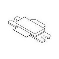
MRF6V12500HR3 Freescale Semiconductor, MRF6V12500HR3 Datasheet - Page 5

MRF6V12500HR3
Manufacturer Part Number
MRF6V12500HR3
Description
FET RF N-CH 1.03GHZ 100V NI-780H
Manufacturer
Freescale Semiconductor
Datasheet
1.MRF6V12500HR5.pdf
(13 pages)
Specifications of MRF6V12500HR3
Transistor Type
N-Channel
Frequency
1.03GHz
Gain
19.7dB
Voltage - Rated
100V
Current - Test
200mA
Voltage - Test
50V
Power - Output
500W
Package / Case
NI-780
Channel Type
N
Channel Mode
Enhancement
Drain Source Voltage (max)
110V
Power Gain (typ)@vds
19.7/18.5dB
Frequency (min)
960MHz
Frequency (max)
1.215GHz
Package Type
NI-780
Pin Count
3
Input Capacitance (typ)@vds
1391@50VpF
Output Capacitance (typ)@vds
697@50VpF
Reverse Capacitance (typ)
0.2@50VpF
Operating Temp Range
-65C to 200C
Drain Efficiency (typ)
62%
Mounting
Screw
Number Of Elements
1
Vswr (max)
10
Screening Level
Military
Lead Free Status / RoHS Status
Lead free / RoHS Compliant
Current Rating
-
Noise Figure
-
Lead Free Status / Rohs Status
Compliant
Available stocks
Company
Part Number
Manufacturer
Quantity
Price
Company:
Part Number:
MRF6V12500HR3
Manufacturer:
FREESCALE
Quantity:
1 400
RF Device Data
Freescale Semiconductor
10000
1000
22
21
20
19
18
17
100
22
21
20
19
18
17
16
15
14
0.1
10
Figure 3. Capacitance versus Drain- -Source Voltage
1
30
30
Figure 5. Pulsed Power Gain and Drain Efficiency
0
V
Pulse Width = 128 μsec, Duty Cycle = 10%
DD
= 50 Vdc, f = 1030 MHz
Figure 7. Pulsed Power Gain versus
200 mA
P
Measured with ±30 mV(rms)ac @ 1 MHz
V
10
P
I
V
out
GS
out
DQ
V
Pulse Width = 128 μsec, Duty Cycle = 10%
DS
DD
, OUTPUT POWER (WATTS) PULSED
, OUTPUT POWER (WATTS) PULSED
= 0 Vdc
= 800 mA
, DRAIN--SOURCE VOLTAGE (VOLTS)
versus Output Power
= 50 Vdc, I
100
100
Output Power
400 mA
G
20
ps
DQ
η
600 mA
= 200 mA, f = 1030 MHz
D
30
TYPICAL CHARACTERISTICS
40
C
C
C
oss
iss
rss
1000
1000
50
80
70
60
50
40
30
20
10
0
160
140
120
100
22
21
20
19
18
17
16
15
14
13
12
80
60
40
20
62
61
60
59
58
57
56
55
54
53
52
51
50
49
0
30
30
0
P1dB = 57.1 dBm (511 W)
I
Pulse Width = 128 μsec
Duty Cycle = 10%
DQ
V
f = 1030 MHz, Pulse Width = 128 μsec
= 200 mA, f = 1030 MHz
DD
Figure 6. Pulsed Output Power versus
Figure 8. Pulsed Power Gain versus
= 50 Vdc, I
P3dB = 57.6 dBm (575 W)
32
P
5
Figure 4. Safe Operating Area
out
P
, OUTPUT POWER (WATTS) PULSED
in
MRF6V12500HR3 MRF6V12500HSR3
DQ
, INPUT POWER (dBm) PULSED
P
V
Pulse Width = 128 μsec, Duty Cycle = 10%
100
out
34
= 200 mA
DD
Output Power
= 525 W
Input Power
DUTY CYCLE (%)
10
= 50 Vdc, I
V
DD
= 30 V
P
36
out
DQ
= 475 W
15
= 200 mA, f = 1030 MHz
35 V
38
40 V
P
out
45 V
20
= 500 W
40
50 V
Actual
Ideal
1000
25
42
5


