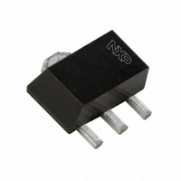
BFQ149,115 NXP Semiconductors, BFQ149,115 Datasheet - Page 2

BFQ149,115
Manufacturer Part Number
BFQ149,115
Description
TRANS PNP 15V 100MA SOT89
Manufacturer
NXP Semiconductors
Datasheet
1.BFQ149115.pdf
(7 pages)
Specifications of BFQ149,115
Package / Case
SC-62, SOT-89, TO-243 (3 Leads + Tab)
Mounting Type
Surface Mount
Power - Max
1W
Current - Collector (ic) (max)
100mA
Voltage - Collector Emitter Breakdown (max)
15V
Transistor Type
PNP
Frequency - Transition
5GHz
Dc Current Gain (hfe) (min) @ Ic, Vce
20 @ 70mA, 10V
Noise Figure (db Typ @ F)
3.75dB @ 500MHz
Dc Current Gain Hfe Max
20 @ 70mA @ 10V
Mounting Style
SMD/SMT
Configuration
Single
Transistor Polarity
PNP
Maximum Operating Frequency
5000 MHz (Typ)
Collector- Emitter Voltage Vceo Max
15 V
Emitter- Base Voltage Vebo
3 V
Continuous Collector Current
0.1 A
Power Dissipation
1000 mW
Maximum Operating Temperature
+ 150 C
Lead Free Status / RoHS Status
Lead free / RoHS Compliant
Gain
-
Lead Free Status / Rohs Status
Lead free / RoHS Compliant
Other names
933897220115::BFQ149 T/R::BFQ149 T/R
Available stocks
Company
Part Number
Manufacturer
Quantity
Price
Company:
Part Number:
BFQ149,115
Manufacturer:
NXP
Quantity:
4 500
NXP Semiconductors
DESCRIPTION
PNP transistor in a SOT89 envelope.
It is intended for use in
UHF applications such as broadband
aerial amplifiers (30 to 860 MHz) and
in microwave amplifiers such as radar
systems, spectrum analysers, etc.,
using SMD technology.
QUICK REFERENCE DATA
LIMITING VALUES
In accordance with the Absolute Maximum System (IEC 134).
Note
1. T
V
I
P
h
f
G
F
V
V
V
I
I
P
T
T
SYMBOL
SYMBOL
C
T
C
CM
FE
stg
j
CEO
tot
CBO
CEO
EBO
tot
PNP 5 GHz wideband transistor
UM
s
is the temperature at the soldering point of the collector tab.
collector-base voltage
collector-emitter voltage
emitter-base voltage
DC collector current
peak collector current
total power dissipation
storage temperature
junction temperature
collector-emitter voltage
DC collector current
total power dissipation
DC current gain
transition frequency
maximum unilateral power gain
noise figure
PARAMETER
PARAMETER
PINNING
PIN
1
2
3
Rev. 03 - 28 September 2007
open base
up to T
I
I
f = 500 MHz; T
I
f = 500 MHz; T
I
R
T
open emitter
open base
open collector
f
up to T
C
C
C
C
amb
s
emitter
collector
base
= 70 mA; V
= 75 mA; V
= 50 mA; V
= 50 mA; V
= 60
1 MHz
Code: FG
= 25 C
DESCRIPTION
s
s
= 135 C (note 1)
= 135 C (note 1)
f = 500 MHz;
CONDITIONS
CONDITIONS
CE
CE
j
CE
amb
CE
= 25 C
= 10 V; T
= 10 V;
= 10 V;
= 10 V;
= 25 C
j
= 25 C 20
4
MIN.
65
MIN.
Fig.1 SOT89.
3
Product specification
50
5
12
3.75
TYP.
1
150
150
2
20
15
3
100
150
MAX.
BFQ149
1
1
MAX. UNIT
15
100
2 of 7
V
V
V
mA
mA
W
C
C
UNIT
V
mA
W
GHz
dB
dB


