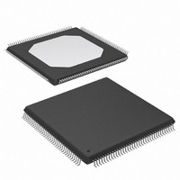
XC3S50-4TQG144C Xilinx Inc, XC3S50-4TQG144C Datasheet - Page 116

XC3S50-4TQG144C
Manufacturer Part Number
XC3S50-4TQG144C
Description
FPGA Spartan®-3 Family 50K Gates 1728 Cells 630MHz 90nm Technology 1.2V 144-Pin TQFP
Manufacturer
Xilinx Inc
Series
Spartan™-3r
Datasheet
1.XC3S50-4VQG100C.pdf
(217 pages)
Specifications of XC3S50-4TQG144C
Package
144TQFP
Family Name
Spartan®-3
Device Logic Units
1728
Device System Gates
50000
Maximum Internal Frequency
630 MHz
Typical Operating Supply Voltage
1.2 V
Maximum Number Of User I/os
97
Ram Bits
73728
Number Of Logic Elements/cells
1728
Number Of Labs/clbs
192
Total Ram Bits
73728
Number Of I /o
97
Number Of Gates
50000
Voltage - Supply
1.14 V ~ 1.26 V
Mounting Type
Surface Mount
Operating Temperature
0°C ~ 85°C
Package / Case
144-LQFP
Case
TQFP144
Dc
06+
Lead Free Status / RoHS Status
Lead free / RoHS Compliant
Available stocks
Company
Part Number
Manufacturer
Quantity
Price
Company:
Part Number:
XC3S50-4TQG144C
Manufacturer:
XILINX43
Quantity:
240
Part Number:
XC3S50-4TQG144C
Manufacturer:
XILINX/赛灵思
Quantity:
20 000
Spartan-3 FPGA Family: Pinout Descriptions
Table 78: Pin Behavior After Power-Up, During Configuration (Continued)
116
Notes:
1.
2.
3.
M1
M0
HSWAP_EN
JTAG: JTAG interface pins (pull-up resistor to VCCAUX always active during configuration, regardless of HSWAP_EN pin)
TDI
TMS
TCK
TDO
VCCO: I/O bank output voltage supply pins
VCCO_4
(for DUAL pins)
VCCO_5
(for DUAL pins)
VCCO_#
VCCAUX: Auxiliary voltage supply pins
VCCAUX
VCCINT: Internal core voltage supply pins
VCCINT
GND: Ground supply pins
GND
Pin Name
#= I/O bank number, an integer from 0 to 7.
(I) = input, (O) = output, (OD) = open-drain output, (I/O) = bidirectional, (I/OD) = bidirectional with open-drain output. Open-drain
output requires pull-up to create logic High level.
drive or tie HSWAP_EN Low.
Shaded cell indicates that the pin is high-impedance during configuration. To enable a soft pull-up resistor during configuration,
Same voltage
HSWAP_EN
as external
VCCO_5
VCCO_#
TDO (O)
interface
M1=0 (I)
M0=0 (I)
<0:0:0>
TMS (I)
Master
TCK (I)
TDI (I)
+2.5V
+1.2V
GND
(I)
Serial Modes
Same voltage
HSWAP_EN
Configuration Mode Settings <M2:M1:M0>
as external
VCCO_5
VCCO_#
TDO (O)
interface
M1=1 (I)
M0=1 (I)
<1:1:1>
TMS (I)
TCK (I)
TDI (I)
Slave
+2.5V
+1.2V
GND
(I)
www.xilinx.com
Same voltage
Same voltage
HSWAP_EN
as external
as external
SelectMap Parallel Modes
VCCO_#
TDO (O)
interface
interface
M1=1 (I)
M0=1 (I)
<0:1:1>
TMS (I)
Master
TCK (I)
TDI (I)
+2.5V
+1.2V
GND
(I)
Same voltage
Same voltage
HSWAP_EN
as external
as external
VCCO_#
TDO (O)
interface
interface
M1=1 (I)
M0=0 (I)
<1:1:0>
TMS (I)
TCK (I)
TDI (I)
Slave
+2.5V
+1.2V
GND
(I)
HSWAP_EN
JTAG Mode
VCCO_4
VCCO_5
VCCO_#
TDO (O)
M1=0 (I)
M0=1 (I)
<1:0:1>
TMS (I)
TCK (I)
DS099-4 (v2.5) December 4, 2009
TDI (I)
+2.5V
+1.2V
GND
(I)
Product Specification
Configuration
HswapenPin
Bitstream
TmsPin
Option
TdoPin
TckPin
M1Pin
M0Pin
TdiPin
R


