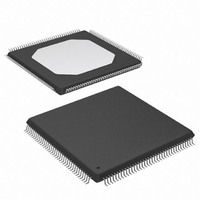
XC3S50-4TQG144C Xilinx Inc, XC3S50-4TQG144C Datasheet - Page 36

XC3S50-4TQG144C
Manufacturer Part Number
XC3S50-4TQG144C
Description
FPGA Spartan®-3 Family 50K Gates 1728 Cells 630MHz 90nm Technology 1.2V 144-Pin TQFP
Manufacturer
Xilinx Inc
Series
Spartan™-3r
Datasheet
1.XC3S50-4VQG100C.pdf
(217 pages)
Specifications of XC3S50-4TQG144C
Package
144TQFP
Family Name
Spartan®-3
Device Logic Units
1728
Device System Gates
50000
Maximum Internal Frequency
630 MHz
Typical Operating Supply Voltage
1.2 V
Maximum Number Of User I/os
97
Ram Bits
73728
Number Of Logic Elements/cells
1728
Number Of Labs/clbs
192
Total Ram Bits
73728
Number Of I /o
97
Number Of Gates
50000
Voltage - Supply
1.14 V ~ 1.26 V
Mounting Type
Surface Mount
Operating Temperature
0°C ~ 85°C
Package / Case
144-LQFP
Case
TQFP144
Dc
06+
Lead Free Status / RoHS Status
Lead free / RoHS Compliant
Available stocks
Company
Part Number
Manufacturer
Quantity
Price
Company:
Part Number:
XC3S50-4TQG144C
Manufacturer:
XILINX43
Quantity:
240
Part Number:
XC3S50-4TQG144C
Manufacturer:
XILINX/赛灵思
Quantity:
20 000
Spartan-3 FPGA Family: Functional Description
Their relative timing in the Low Frequency Mode is shown in
Figure
not available when operating in the High Frequency mode.
(See the description of the DLL_FREQUENCY_MODE
attribute in
90°, see the
Basic Frequency Synthesis Outputs of the DLL
Component
The DLL component provides basic options for frequency
multiplication and division in addition to the more flexible
synthesis capability of the DFS component, described in a
later section. These operations result in output clock signals
with frequencies that are either a fraction (for division) or a
multiple (for multiplication) of the incoming clock frequency.
The CLK2X output produces an in-phase signal that is twice
the frequency of CLKIN. The CLK2X180 output also dou-
bles the frequency, but is 180° out-of-phase with respect to
CLKIN. The CLKDIV output generates a clock frequency
that is a predetermined fraction of the CLKIN frequency.
The CLKDV_DIVIDE attribute determines the factor used to
divide the CLKIN frequency. The attribute can be set to var-
ious values as described in
synthesis outputs are described in
timing in the Low Frequency Mode is shown in
The CLK2X and CLK2X180 outputs are not available when
operating in the High Frequency mode. (See the description
of the DLL_FREQUENCY_MODE attribute in
Duty Cycle Correction of DLL Clock Outputs
The CLK2X
ordinarily exhibit a 50% duty cycle – even if the incoming
CLKIN signal has a different duty cycle. Fifty-percent duty
cycle means that the High and Low times of each clock
cycle are equal. The DUTY_CYCLE_CORRECTION
attribute determines whether or not duty cycle correction is
applied to the CLK0, CLK90, CLK180 and CLK270 outputs.
If DUTY_CYCLE_CORRECTION is set to TRUE, then the
duty cycle of these four outputs is corrected to 50%. If
DUTY_CYCLE_CORRECTION is set to FALSE, then these
outputs exhibit the same duty cycle as the CLKIN signal.
Figure 20
signals to those of the CLKIN signal.
1. The CLK2X output generates a 25% duty cycle clock at the same frequency as the CLKIN signal until the DLL has achieved lock.
2. The duty cycle of the CLKDV outputs may differ somewhat from 50% (i.e., the signal will be High for less than 50% of the period) when
36
54
the CLKDV_DIVIDE attribute is set to a non-integer value and the DLL is operating in the High Frequency mode.
20. The CLK90, CLK180 and CLK270 outputs are
compares the characteristics of the DLL’s output
Table
(1)
Phase Shifter (PS), page 38
, CLK2X180, and CLKDV
16.) For control in finer increments than
Table
16. The basic frequency
Table
(2)
15. Their relative
section.
output signals
Table
Figure
17.)
www.xilinx.com
20.
Phase:
Input Signal (40% Duty Cycle)
Output Signal - Duty Cycle is Always Corrected
Output Signal - Attribute Corrects Duty Cycle
Notes:
1.
CLK2X180
CLKDV
Figure 20: Characteristics of the DLL Clock Outputs
DUTY_CYCLE_CORRECTION = FALSE
CLK180
CLK270
DUTY_CYCLE_CORRECTION = TRUE
CLK180
CLK270
CLK2X
CLK90
CLK90
The DLL attribute CLKDV_DIVIDE is set to 2.
CLKIN
CLK0
CLK0
(1)
0
o
90
o
180
t
o
DS099-2 (v2.5) December 4, 2009
270
o
0
o
90
Product Specification
o
180
o
270
DS099-2_10_051907
o
0
o
R


